Wafer-on-Wafer Bonding Breaks AI's Bandwidth Wall
Wafer-on-Wafer Bonding Breaks AI's Bandwidth Wall
Why Quantum Computers Need 1,000 Qubits for One
TPM 2.0 and Pluton: Hardware Root of Trust Explained
Why Quantum Computing Bet on One Qubit Design

P4 Programmable Switches Rewriting Networks at Tbps
Intel TSX Failed. Can ARM Fix Transactional Memory?
TL;DR: Chiplet architecture is revolutionizing semiconductor design by breaking monolithic processors into specialized, mix-and-match modules. This modular approach bypasses Moore's Law limitations while offering superior manufacturing yields, cost flexibility, and performance scaling for AI, data centers, and future computing.
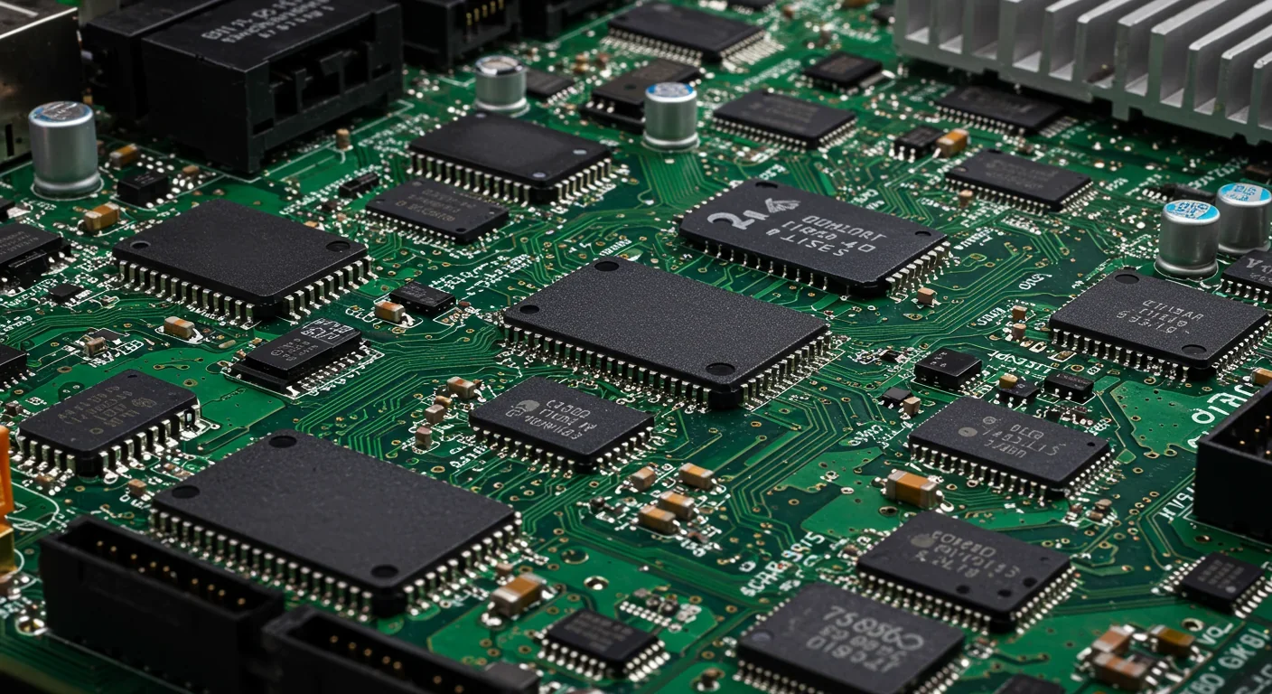
The semiconductor industry is experiencing its most significant architectural shift in decades. After fifty years of shrinking transistors to boost performance, chipmakers are fundamentally changing how they build processors. Instead of cramming everything onto one massive silicon die, they're breaking chips into specialized modules called chiplets, then connecting them like digital building blocks.
This isn't just clever engineering. It's a strategic pivot that could determine which companies dominate computing for the next generation. AMD's chiplet-based processors already power some of the world's fastest supercomputers, while Intel has bet its foundry business on advanced packaging technologies that make chiplets practical. The question isn't whether chiplets will replace monolithic designs, but how fast the transition will happen and who will control the standards.
For most of computing history, progress followed a predictable pattern. Every two years, manufacturers doubled the number of transistors they could fit on a chip by making each transistor smaller. Gordon Moore's 1965 observation became a self-fulfilling prophecy that drove exponential performance gains for half a century.
But physics doesn't care about industry roadmaps. As transistors approach atomic dimensions, quantum effects start causing problems. Electrons tunnel through barriers they should respect. Heat becomes impossible to dissipate. The cost of building fabs capable of producing chips at cutting-edge nodes has skyrocketed to over $20 billion per facility, pricing out all but the wealthiest companies.
Recent analysis shows we're hitting fundamental limits that no amount of engineering cleverness can overcome. You can't go smaller than an atom. Traditional scaling is reaching its natural conclusion, and the semiconductor industry needed a new playbook.
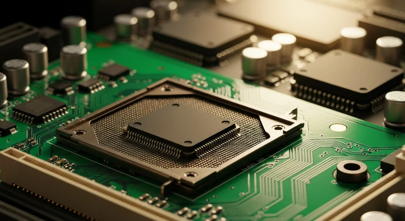
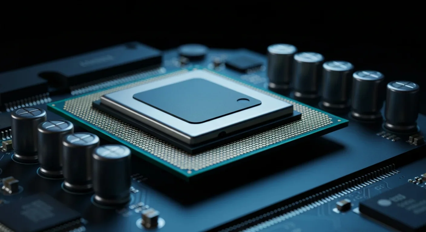
Think of a traditional processor as a single massive building where every department shares the same foundation. A chiplet design is more like a campus, where specialized buildings connect through high-speed walkways. Each chiplet handles one job exceptionally well, whether that's processing calculations, managing memory, or handling input/output operations.
Chiplet architecture breaks monolithic processors into specialized modules that can be mixed, matched, and optimized independently - fundamentally changing how we design computing systems.
AMD's Ryzen processors pioneered this approach in consumer products, using separate chiplets for CPU cores and I/O functions connected through their Infinity Fabric interconnect. Apple's M1 chip, while technically a system-on-chip, incorporates principles of heterogeneous integration that mirror chiplet philosophy by combining different silicon types optimized for specific tasks.
The technical magic happens in how these pieces connect. Silicon interposers create ultra-short electrical pathways between chiplets, while 3D stacking technologies like Intel's Foveros stack chiplets vertically to minimize distance and maximize bandwidth. These aren't simple wire connections; they're sophisticated communication highways that move terabytes of data per second between chiplets.
Manufacturing economics make chiplet architecture compelling beyond pure performance. When you fabricate a massive monolithic chip, a single microscopic defect anywhere on the die ruins the entire piece of silicon. As chips get larger, the probability of defects increases exponentially.
Smaller chiplets have dramatically better yields because defects are less likely to occur in smaller areas. If one chiplet in a batch has a flaw, you've wasted a small piece of silicon rather than an entire processor. This matters more as cutting-edge manufacturing nodes become eye-wateringly expensive.
There's also flexibility in process selection. Different chiplets can be manufactured using different technologies optimized for their specific function. Your high-performance CPU cores might use bleeding-edge 3-nanometer processes, while your I/O chiplet uses a cheaper, more mature 14-nanometer node perfectly adequate for its less demanding task. You pay premium prices only for the components that absolutely need cutting-edge performance.
"The chiplet market could reach $411 billion by 2035, driven by economic advantages combined with insatiable demand for computing power in AI, data centers, and edge computing."
- Microwave Journal Market Analysis
The theoretical benefits of chiplets only matter if they deliver in practice. AMD's EPYC Rome processors, based on chiplet architecture, demonstrated that modular designs could compete with and often exceed monolithic chips in real-world workloads. These processors combine up to eight CPU chiplets with a central I/O die, delivering up to 64 cores in configurations that would be economically impossible with traditional monolithic designs.
Performance data shows chiplet designs achieving remarkable results. AMD's EPYC 9634 delivers exceptional performance in AI and machine learning workloads, demonstrating that inter-chiplet communication overhead can be minimized through clever design. The processor balances high core counts with memory bandwidth in ways that would challenge monolithic architectures.
Intel has responded with its own chiplet strategies. Their advanced packaging roadmap emphasizes sophisticated interconnect technologies as core competencies. The company is positioning its foundry business around the assumption that chiplet-based designs will dominate future computing.
Heterogeneous integration has become a critical capability. Modern processors increasingly combine silicon chiplets with compound semiconductors for RF functions, specialized AI accelerators, and even optical interconnects for ultra-high-bandwidth communication.

The biggest obstacle to widespread chiplet adoption isn't technical, it's political. For chiplets to reach their full potential, different manufacturers need to build components that work together seamlessly. That requires industry-wide standards, and getting competitors to agree on technical specifications is notoriously difficult.
UCIe (Universal Chiplet Interconnect Express) represents the industry's most ambitious standardization effort. Led by a consortium including Intel, AMD, Arm, TSMC, and Samsung, UCIe aims to create an open standard for die-to-die connectivity that would allow mix-and-match chiplet ecosystems.
The UCIe specification defines physical, electrical, and protocol layers for chiplet communication, attempting to do for chiplets what USB did for peripherals. Version 1.0 supports up to 2 terabytes per second of bandwidth using a compact physical interface that minimizes power consumption.
UCIe aims to create an open standard for chiplet connectivity, enabling a mix-and-match ecosystem where components from different manufacturers work seamlessly together.
Recent updates have increased speeds even further, with next-generation UCIe targeting even higher bandwidth to support demanding AI and high-performance computing applications. Optical I/O integration is being explored as a complement to electrical connections for scenarios requiring extreme data movement.
But standards battles are never simple. Companies want to shape specifications to favor their existing intellectual property and manufacturing capabilities. Business analysis of chiplet ecosystems shows complex negotiations over licensing, intellectual property rights, and ecosystem control that will determine which standards achieve broad adoption.
Chiplet architecture solves some problems while creating new ones. Inter-chiplet communication latency remains higher than on-die interconnects, even with advanced packaging. When data needs to travel between chiplets, it crosses physical boundaries that introduce delays measured in nanoseconds, tiny delays that matter in high-performance computing.
Power management becomes significantly more complex when multiple chiplets operate independently. Each chiplet may have different power requirements and thermal characteristics, requiring sophisticated coordination to prevent hotspots and optimize overall system efficiency. You can't simply treat a chiplet system like a traditional monolithic processor when managing power states.
Design verification and testing present new challenges. With monolithic designs, you verify the entire chip as one unit. Chiplet systems require verifying not just individual chiplets but all possible interactions between them, exponentially increasing testing complexity. The industry is developing new methodologies and tools specifically for chiplet validation.
Resource management across chiplets requires new approaches. How do you allocate cache coherency, memory bandwidth, and processing resources when they're physically distributed across multiple dies? Software and firmware need to understand chiplet topology to optimize performance.
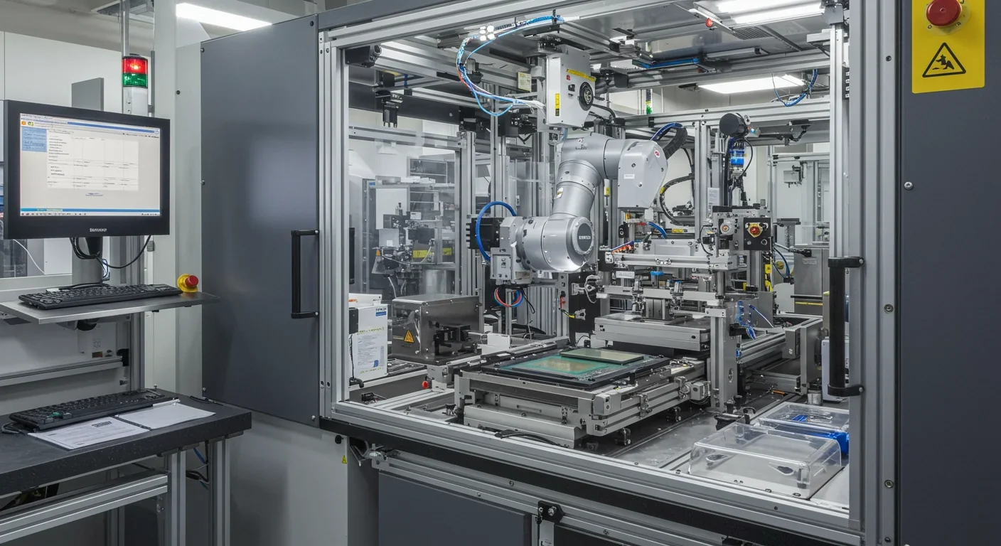
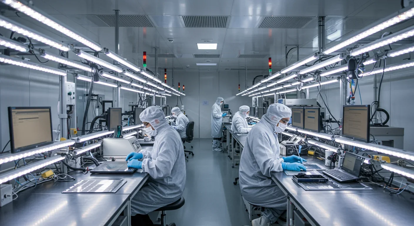
Chiplet architecture is transforming semiconductor manufacturing beyond just chip design. Advanced packaging has become as critical as lithography, requiring massive investments in new fabrication capabilities. Companies that previously focused on silicon manufacturing now need expertise in 3D stacking, interposer fabrication, and ultra-precise assembly.
Supply chains are becoming more complex and specialized. Top chiplet manufacturers are emerging across different parts of the ecosystem, some focusing on specific chiplet types, others on interconnect technologies, and still others on packaging and assembly services.
This creates opportunities for companies that can't afford to build leading-edge fabs but can design excellent specialized chiplets. A small company with innovative AI accelerator designs could build their chiplet at a foundry, then integrate it with CPU chiplets from larger manufacturers using standard interconnects. The barrier to entry for certain types of semiconductor innovation decreases significantly.
DARPA's Common Heterogeneous Integration and IP Reuse Strategies program has accelerated development of chiplet ecosystems by funding open-source chiplet designs and promoting interoperability standards. Government investment recognizes chiplets as strategically important for maintaining semiconductor competitiveness.
Artificial intelligence workloads are driving some of the most aggressive chiplet adoption. Modern AI systems need massive parallel processing combined with enormous memory bandwidth, requirements perfectly suited to chiplet architecture. You can dedicate chiplets to tensor operations while others handle memory management, creating balanced systems optimized for machine learning.
Data centers are embracing chiplet-based processors because they offer customization impossible with monolithic designs. Cloud providers can work with semiconductor companies to create processors with exactly the mix of CPU cores, accelerators, and I/O capabilities their specific workloads require. You're no longer forced to choose from a limited menu of pre-configured processors.
The economic model for hyperscale data centers makes custom chiplet configurations particularly attractive. When you're deploying hundreds of thousands of processors, even small efficiency gains from perfectly matched hardware translate into millions of dollars in reduced power consumption and improved performance.
Edge computing applications benefit differently. Chiplets allow creating diverse product lines from a common library of components, supporting everything from low-power embedded devices to high-performance edge servers without designing each from scratch. Development costs drop while product variety increases.
Chiplet-based architectures introduce new security considerations that didn't exist with monolithic designs. When multiple chiplets communicate across physical boundaries, each interface becomes a potential attack surface. Securing inter-chiplet communication requires encryption and authentication mechanisms that add complexity and power consumption.
Supply chain security becomes more challenging when processors incorporate chiplets from multiple sources. How do you verify that every chiplet in a system is authentic and hasn't been tampered with? The industry is developing hardware root-of-trust solutions and secure boot mechanisms specifically for chiplet systems.
"Chiplet architecture allows incorporating dedicated security chiplets with hardware-accelerated encryption and secure enclaves, building security into the fundamental architecture rather than treating it as an add-on."
- Semiconductor Engineering
There's also opportunity in this challenge. Chiplet architecture allows incorporating dedicated security chiplets with hardware-accelerated encryption, secure enclaves, and tamper detection. You can build security into the fundamental architecture rather than treating it as an add-on feature.

Looking forward, chiplet architecture enables possibilities that seemed like science fiction a decade ago. 3D integration is advancing rapidly, with researchers stacking not just two but many layers of chiplets vertically, connected through micro-bumps and through-silicon vias that create essentially three-dimensional processors.
Hybrid integration of different semiconductor materials lets engineers combine silicon with gallium nitride, silicon carbide, and other exotic materials optimized for specific functions. A single package might contain silicon for logic, gallium nitride for power management, and photonic chiplets for optical communication.
The concept of a "processor" is becoming fluid. In a chiplet world, the distinction between CPU, GPU, accelerator, and memory controller blurs. Systems are assembled from functional blocks matched to workload requirements rather than forcing workloads to adapt to fixed processor architectures.
Consumer devices will feel this shift indirectly. Your next smartphone won't advertise its chiplet count, but the technology will enable better battery life, improved AI capabilities, and features that would be impossible or economically impractical with monolithic designs. Technology that starts in data centers and high-performance computing eventually reaches everyday devices.
Investors and companies making technology decisions need to understand that chiplet adoption represents a fundamental platform shift comparable to the transition from mainframes to personal computers or from CPUs to heterogeneous computing. Companies with strong positions in advanced packaging, interconnect technologies, and design tools for chiplet systems will capture value as the industry transitions.
Traditional competitive advantages in leading-edge lithography become less decisive when chiplets allow mixing process nodes. A company with excellent 7-nanometer manufacturing might remain competitive by focusing on specific chiplet types rather than racing to 3-nanometer processes. The competitive landscape is being redrawn.
For enterprise technology buyers, chiplet-based systems offer customization and optimization opportunities previously available only to hyperscalers. As standardization progresses and chiplet marketplaces emerge, companies will be able to specify processors tailored to their exact requirements rather than choosing from commodity options.
Industry analysis suggests chiplet technology will drive the next wave of semiconductor innovation, enabling applications from personalized medicine through custom biocomputing processors to autonomous vehicles with specialized sensor-fusion chiplets to quantum computing interfaces.
The transition to chiplet architecture will reshape how we think about computing at every level. For engineers and technologists, this means developing new skills in system-level design, advanced packaging, and heterogeneous integration. The era of focusing purely on silicon design or purely on PCB design is ending; the future belongs to those who can think across abstraction layers.
Educational institutions are beginning to adapt curricula to emphasize system-level thinking over purely transistor-level design. New design tools and methodologies are emerging specifically for chiplet systems, requiring engineers to master different abstractions than those used for monolithic chips.
For the broader technology industry, chiplet architecture represents both disruption and opportunity. New entrants can compete in specific chiplet niches without the enormous capital requirements of traditional semiconductor manufacturing. Established players must adapt or risk losing relevance as the industry reorganizes around modular design.
The geopolitical dimension matters too. Countries investing in semiconductor self-sufficiency recognize that chiplet technology changes the game. A nation that can't compete in leading-edge lithography might still build competitive systems by excelling in packaging, interconnects, or specialized chiplet designs. The strategic landscape is becoming more complex and multi-dimensional.
Chiplet architecture isn't a temporary workaround for Moore's Law ending; it's a fundamental rethinking of how we build computing systems. By breaking monolithic designs into specialized, interoperable components, the semiconductor industry has found a path to continued performance scaling even as traditional transistor shrinking reaches physical limits.
The transition won't happen instantly. Monolithic designs will persist where they make sense, particularly for cost-sensitive applications or where integration benefits outweigh modular flexibility. But for high-performance computing, AI, data centers, and increasingly for consumer devices, chiplets represent the architectural foundation for the next several decades of innovation.
We're entering an era where processors are assembled like software from libraries of components rather than designed as monolithic units. This shift will democratize certain types of semiconductor innovation while creating new challenges in standardization, security, and system integration. The companies and countries that master chiplet design, advanced packaging, and ecosystem development will define computing's next chapter.
The semiconductor industry has reinvented itself before, and chiplet architecture is its latest evolution. What makes this transition different is that it doesn't fight physics but works with fundamental realities of manufacturing and economics. In breaking the monolithic paradigm, chipmakers have found not just a path forward but potentially a superior approach that could have been adopted earlier if not for the momentum of fifty years of successful scaling.
The revolution in how we build processors is already underway. The question now is how quickly the rest of the technology ecosystem adapts to the possibilities that modular, heterogeneous computing enables.

Saturn's moon Titan may harbour liquid water beneath its frozen crust, kept from freezing by ammonia acting as a natural antifreeze. New Cassini data suggests the interior could be slush with warm water pockets rather than a global ocean, and NASA's Dragonfly mission launching in 2028 aims to investigate whether this exotic environment could support life.

The cerebellum, long dismissed as merely a motor coordinator, forms dense circuits with the prefrontal cortex that shape cognition and emotion. Disruption of these pathways is now linked to schizophrenia, autism, and ADHD, opening new frontiers in diagnosis and non-invasive brain stimulation therapies.

Research shows the sharing economy often increases total resource consumption through the Jevons paradox and rebound effects. Ride-sharing adds billions of vehicle miles, co-working spaces use more energy per worker, and diffused responsibility erodes conservation behavior. Breaking the paradox requires congestion pricing, accountability design, and matching sharing models to appropriate resource types.

Illusory superiority causes most people to rate themselves above average in driving, intelligence, and ethics. This bias is rooted in metacognitive blind spots, shaped by culture, and carries real costs in healthcare, finance, and leadership. Structured feedback and institutional safeguards can help, but require ongoing effort.

Eastern skunk cabbage generates its own body heat through the alternative oxidase pathway, maintaining temperatures up to 35°C above freezing air and melting surrounding snow. This thermogenic ability, shared by roughly 90 plant species worldwide, reveals a level of metabolic sophistication that challenges assumptions about plant passivity.

America has 28 vacant homes for every homeless person, yet homelessness hit record highs in 2024. Speculative investment, geographic mismatches, and political barriers explain the paradox, while Finland and Vienna show that Housing First and social housing models can work when the political will exists.
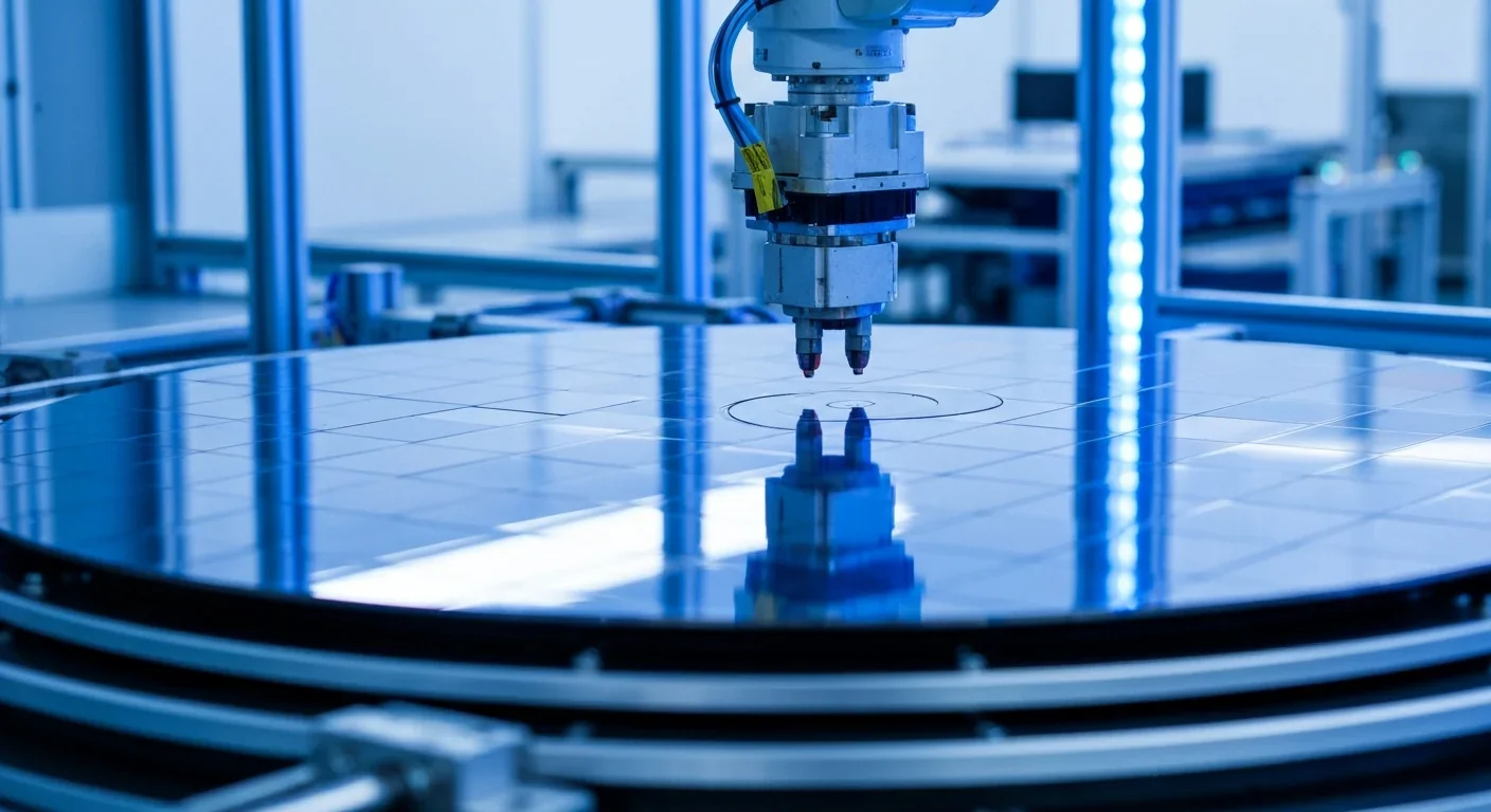
Wafer-on-wafer bonding fuses logic and memory silicon at the atomic level, delivering up to 100x interconnect density over traditional packaging. TSMC, Intel, and Samsung are racing to commercialize the technology as AI chips hit the memory bandwidth wall.

Loading featured articles...