Wafer-on-Wafer Bonding Breaks AI's Bandwidth Wall
Wafer-on-Wafer Bonding Breaks AI's Bandwidth Wall
Why Quantum Computers Need 1,000 Qubits for One
TPM 2.0 and Pluton: Hardware Root of Trust Explained
Why Quantum Computing Bet on One Qubit Design

P4 Programmable Switches Rewriting Networks at Tbps
Intel TSX Failed. Can ARM Fix Transactional Memory?
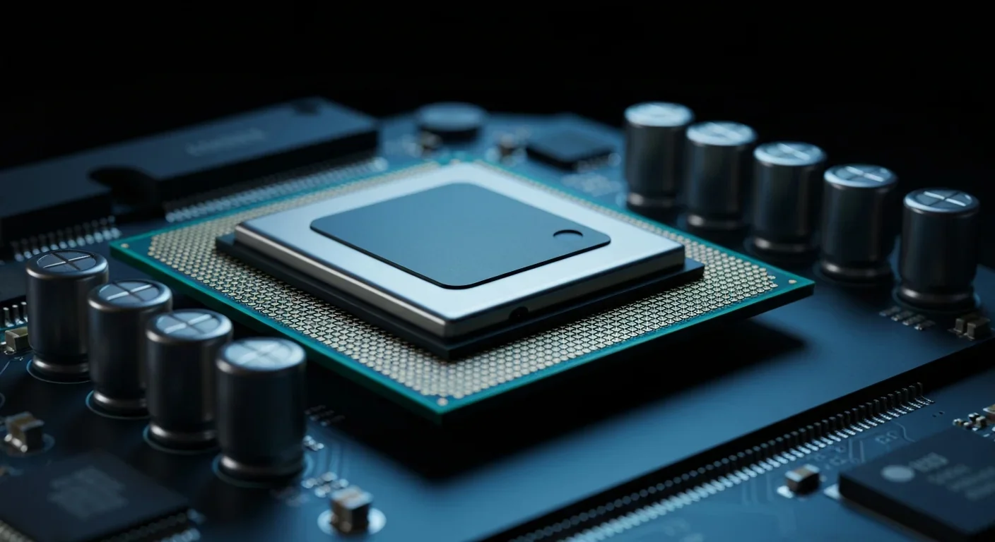
TL;DR: Cerebras Systems defied semiconductor industry consensus by building the world's largest processor - a 46,225 square millimeter wafer-scale chip with up to 900,000 cores. Through innovative redundancy and on-chip memory delivering 20 petabytes per second bandwidth, they've achieved performance advantages of 5-210x over GPU clusters while dramatically simplifying AI development.
In 2015, a team of engineers gathered in a small office in Los Altos, California, to discuss what everyone else in the semiconductor industry considered impossible. They wanted to build a computer chip from an entire silicon wafer - 46,225 square millimeters of continuous silicon - when conventional wisdom said you couldn't manufacture anything larger than about 800 square millimeters without catastrophic failure. Eight years later, Cerebras Systems has shipped three generations of the world's largest processor, fundamentally challenging how we think about AI computing.
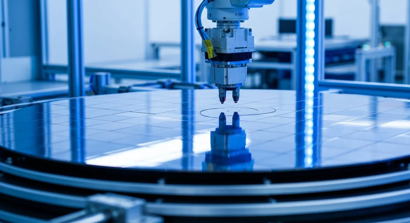
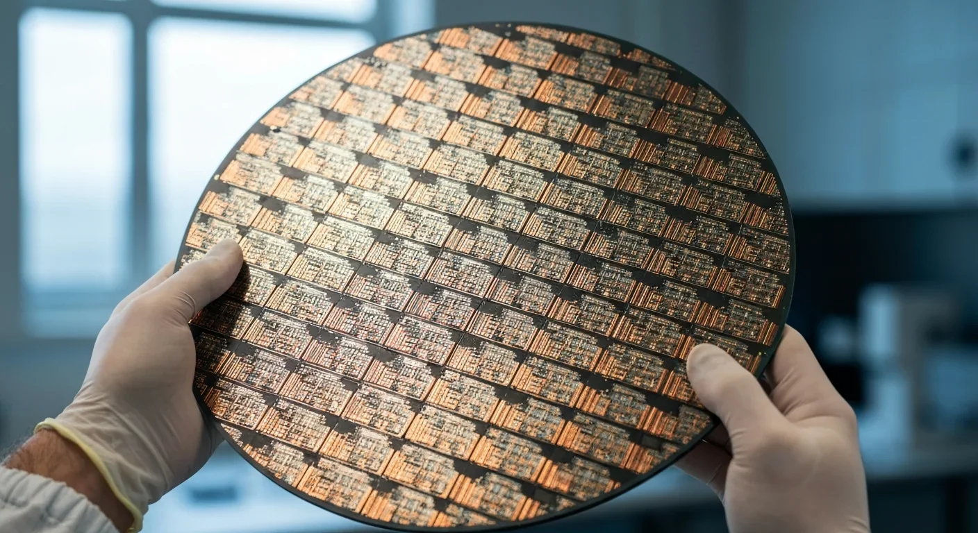
Manufacturing a traditional chip is a delicate balance of probability and precision. Silicon wafers - the circular platters from which chips are cut - inevitably contain microscopic defects. That's why foundries like TSMC divide each wafer into hundreds of small chips: if a defect ruins one chip, you lose only that piece, not the entire wafer.
The math is unforgiving. A wafer might have 0.09 defects per square centimeter - TSMC's 7nm process specification. For an NVIDIA H100 GPU at roughly 815 square millimeters, that's manageable. But scale up to 46,225 square millimeters? You're mathematically guaranteed to have dozens of defects across the wafer. Conventional wisdom said the entire chip would be dead on arrival.
Cerebras didn't try to eliminate defects. Instead, they built around them. Their Wafer Scale Engine includes redundant cores throughout the chip. When a defect appears during manufacturing, the system simply routes around it, like traffic diverting around a closed road. By making each core just 0.05 square millimeters - tiny compared to traditional processors - the company reduced the area lost per defect to almost nothing. This approach gives Cerebras roughly 164 times higher fault tolerance than competing GPUs.
By making each core just 0.05 square millimeters, Cerebras achieved roughly 164 times higher fault tolerance than competing GPUs - turning the impossible physics of wafer-scale manufacturing into a solvable engineering problem.
"Working with TSMC, Cerebras has repurposed the scribe lines - normally just the cutting guides between individual chips - as wires that connect one die to another," explains the technical documentation. This created an on-wafer communication fabric that lets 850,000 cores (in the WSE-2) or 900,000 cores (in the WSE-3) work together as a unified processor.
Think about how computers normally work. Your processor sits on one side of a circuit board. Memory sits on the other side. Data constantly shuttles back and forth across centimeters of copper traces, package boundaries, and connector pins. This "von Neumann bottleneck" has plagued computing since the 1940s, and it's getting worse as AI models grow exponentially.
GPUs try to solve this with High Bandwidth Memory (HBM) - expensive memory chips stacked directly atop the processor. NVIDIA's H100 achieves about 3 terabytes per second of memory bandwidth this way. It's impressive until you see what Cerebras achieved.
The WSE-2 integrates 40 gigabytes of SRAM directly onto the processor die. Not stacked on top. Not connected through an interposer. Literally part of the same piece of silicon. This delivers 20 petabytes per second of memory bandwidth - roughly 6,600 times more than the H100. The implications are staggering.
For AI training, memory bandwidth often matters more than raw compute power. Large language models constantly fetch weights and activations from memory. On a GPU cluster, much of your time is spent waiting for data to arrive. On the WSE, the entire model can fit in on-chip memory with essentially zero latency.
"The WSE's dataflow architecture eliminates the memory latency and bandwidth bottlenecks commonly seen in GPUs, achieving a 210x performance boost over an H100 GPU."
- Researchers from Rice University and TotalEnergies
Real-world results validate this advantage. Researchers from Rice University and TotalEnergies tested the WSE against NVIDIA's H100 for carbon capture simulations - a demanding computational fluid dynamics workload. The WSE delivered a 210x performance advantage, hitting 1.217 petaflops on a single node. The dataflow architecture eliminated memory bottlenecks entirely.
Here's where things get interesting beyond the hardware specs. Training a massive AI model on a GPU cluster isn't just a hardware challenge - it's a software nightmare.
You need to partition the model across hundreds or thousands of individual GPUs. You need to orchestrate communication between them. You need to handle failures when individual GPUs drop offline. You need to manage distributed memory, synchronize gradients, and debug across a cluster. Training a 175-billion-parameter model on 4,000 GPUs requires about 20,000 lines of code.
On Cerebras? The same task takes 565 lines of code and finishes in one day.
This isn't marketing spin. When your entire model fits on a single chip with unified memory, you eliminate the entire distributed computing layer. No more multi-node synchronization. No more network optimization. No more debugging why GPU 2,847 in rack 43 is behaving differently than the others.
GSK reported cutting molecular dynamics training from 14 days to 7 hours on their first-generation CS-1 system. Argonne National Laboratory reduced experiment turnaround time by 300x. These aren't incremental improvements - they're order-of-magnitude leaps that change what's computationally feasible.
A Cerebras CS-2 system costs between $2 million and $3 million. Before you gasp at the price tag, consider what you're replacing.
An equivalent GPU cluster might need hundreds of H100s at roughly $30,000 each, plus networking equipment, additional power infrastructure, cooling systems, and rack space. You're looking at similar capital costs, but dramatically higher operational expenses. The CS-2 draws 15-20 kilowatts and fits in one-third of a standard rack. A comparable GPU cluster might fill multiple racks and consume substantially more power.

Recent comparisons show Cerebras delivering 3,000 tokens per second at $0.75 per million tokens for inference workloads, while NVIDIA's latest Blackwell architecture on eight GB200 GPUs manages 650 tokens per second at $0.50 per million. Cerebras's price-performance ratio works out to roughly 4,000 versus 1,300 - three times better despite the higher per-token cost.
Total cost of ownership becomes favorable when you account for the smaller physical footprint, lower cooling requirements, and dramatically reduced software development costs. You're not paying engineers to optimize distributed training frameworks - you're training models.
Dissipating 20 kilowatts from a single chip is no small feat. A typical high-end desktop processor might consume 200-300 watts. Cerebras is removing 60-100 times more heat from a single point.
The solution required rethinking traditional packaging entirely. Instead of mounting the chip in a conventional package, Cerebras places the entire wafer on a printed circuit board with a flexible membrane between the silicon and the board. This membrane accommodates differential thermal expansion - silicon and PCB materials expand at different rates when heated, and rigid connections would fracture under the stress.
A custom heat exchanger sits directly atop the wafer, with specialized liquid cooling removing the thermal load. The system includes over 300 voltage regulation modules to deliver stable power across the massive die. This isn't something you could build with off-the-shelf components; it required co-designing the silicon, packaging, cooling, and power delivery as an integrated system.
Wafer-scale processors aren't for everyone, but they've found a natural fit in several domains. The U.S. Department of Energy labs use them for scientific computing and large-scale simulations. Pharmaceutical companies like GlaxoSmithKline and AstraZeneca deploy them for drug discovery and genetic research. TotalEnergies uses them for reservoir simulation and carbon capture modeling.
Financial institutions have also adopted the technology, though they tend not to publicize the details. The common thread? Organizations that need to train or run very large models where the total cost and time-to-result matter more than the per-unit hardware cost.
Cerebras reported revenue growth from $78.7 million in 2023 to an estimated $500 million in 2024 - a 6.3x increase that signals real market traction beyond early adopters.
Cerebras reported revenue growth from $78.7 million in 2023 to an estimated $500 million in 2024 - a 6.3x increase suggesting real market traction. The company went public in 2024, giving the market a clearer view of the business model.
NVIDIA hasn't stood still. Their Blackwell architecture, announced in 2024, represents a significant step forward in GPU performance. The GB200 combines two GPU dies with aggressive packaging and high-bandwidth interconnects.

But here's what's remarkable: even against NVIDIA's latest refresh, Cerebras maintains a substantial advantage for specific workloads. The WSE-3 delivers roughly 3.5 times the FP8 performance of the H100 and 1.1 times the B200. For inference, the gap is even larger - a 5x throughput advantage over Blackwell.
This suggests the wafer-scale advantage isn't a temporary quirk that disappears with the next GPU generation. The architectural differences run deeper than process node or transistor count. By eliminating inter-chip communication entirely, Cerebras sidesteps a fundamental bottleneck that even the best GPU clusters can't fully overcome.
Before we get too carried away, let's acknowledge the constraints. The WSE is highly specialized. It excels at dense linear algebra and large-scale neural networks. It's not replacing your laptop processor or gaming GPU. For general-purpose computing, the traditional chip model works fine.
Manufacturing remains expensive and complex. Only TSMC currently has the process maturity and defect density low enough to make wafer-scale economical. You can't fab these chips anywhere else. That creates supply chain concentration risk.
The chips also require specialized infrastructure. You can't just drop a CS-3 into a standard server rack and expect it to work. The cooling, power delivery, and networking all need custom engineering. For smaller organizations or those without dedicated infrastructure teams, this is a significant barrier to adoption.
The idea of wafer-scale integration isn't new. In the 1980s, several companies tried and failed to commercialize the approach. Trilogy Systems famously spent over $200 million trying to build a wafer-scale computer before collapsing in 1985. Anamartic and others followed similar paths to similar failures.
What changed? Manufacturing precision. When TSMC's 7nm process can maintain 0.09 defects per square centimeter across an entire wafer - down from much higher rates in earlier decades - suddenly the economics shift. Cerebras also benefited from three decades of accumulated knowledge about redundancy, error correction, and fault-tolerant architectures.
"When we started on this journey eight years ago, everyone said wafer-scale processors were a pipe dream. We could not be more proud to be introducing the third-generation of our groundbreaking wafer-scale AI chip."
- Andrew Feldman, CEO and co-founder of Cerebras Systems
Sometimes an idea isn't wrong, just early. Wafer-scale integration required semiconductor manufacturing to reach a maturity level that simply didn't exist in the 1980s. Cerebras built the right architecture at the right moment in manufacturing history.
Step back from the technical details and you see a larger trend. For decades, general-purpose processors drove progress. Intel's x86 chips ran everything from laptops to servers. Then GPUs proved that specialized silicon could massively outperform CPUs for parallel workloads. Now we're seeing further specialization: AI accelerators, tensor processors, wafer-scale engines.
This mirrors what happened in earlier industrial revolutions. Early factories used a single large steam engine with belts and pulleys distributing power throughout the building. Then electric motors became cheap enough to put one on every machine. Specialization won because it eliminated transmission losses and allowed each machine to optimize independently.
The same principle applies to computing. As AI models grow larger and more important, organizations are willing to invest in specialized hardware that eliminates bottlenecks. The question isn't whether specialized processors make sense - the question is which architectures will dominate which workloads.

If Cerebras's approach proves broadly successful, it could reshape the AI hardware landscape in several ways.
First, it challenges NVIDIA's near-monopoly on AI training hardware. When one company controls 90%+ of a critical technology stack, prices tend to stay high and innovation can slow. Credible competition forces everyone to innovate faster and price more competitively.
Second, it suggests that software simplicity might matter more than raw peak performance. The 97% code reduction for large language models isn't just a convenience - it means smaller teams can train frontier models. That could democratize access to cutting-edge AI capabilities.
Third, it validates the idea that domain-specific architectures can beat general-purpose hardware by enormous margins. If you're running a specific workload at scale, paying for custom silicon makes economic sense. We'll likely see more specialized processors targeting other domains: genomics, climate modeling, financial simulation.
There's a sustainability argument here that doesn't get enough attention. Data centers already consume roughly 1-2% of global electricity, and AI training is one of the fastest-growing components of that load.
A CS-3 system consuming 20 kilowatts that replaces a cluster consuming 60-80 kilowatts doesn't just save operating costs - it reduces carbon emissions. When you multiply that across thousands of systems, the environmental impact becomes significant.
When training time drops from weeks to days, you're not just saving time - you're consuming dramatically less total energy while enabling more experimentation that could accelerate progress toward more efficient AI architectures.
More importantly, the training time reduction changes the equation. If you can train a model in one day instead of weeks, you're not just saving time - you're consuming dramatically less total energy. The faster turnaround also enables more experimentation, which could accelerate progress toward more efficient AI architectures.
Cerebras isn't resting on three generations of success. The company continues pushing the boundaries of wafer-scale design. Future iterations will likely increase core counts, improve power efficiency, and expand the range of workloads that benefit from the architecture.
The broader question is whether other companies will follow. Google's TPUs already represent a move toward specialized AI silicon. Amazon is designing custom chips for AWS. Even Apple has invested heavily in neural engines for their devices.
We're witnessing a Cambrian explosion of chip architectures, all optimized for different points in the performance-cost-power design space. Some will thrive. Others will fade away. But the era of one-size-fits-all processors is definitively over.
Behind all the technical specifications and performance benchmarks, there's a story about persistence against consensus reality. When Andrew Feldman and his team started Cerebras in 2015, virtually every semiconductor expert told them wafer-scale integration couldn't work. The physics was wrong. The economics didn't make sense. The yield would be terrible.
They built it anyway. Three generations of successful products later, the "impossible" chip is helping pharmaceutical companies design new drugs, enabling national labs to run climate simulations, and pushing the boundaries of what large language models can achieve.
Sometimes progress requires ignoring the experts and building the thing everyone says can't exist. The WSE exists not because the conventional wisdom changed, but because a small team refused to accept it.
If you're not running an AI research lab or a pharmaceutical company, you might wonder why any of this matters. The answer is that today's specialized AI hardware enables tomorrow's applications.
The drug discovery speedups at GSK and AstraZeneca could mean new treatments reaching patients years earlier. Climate models running 100x faster could improve weather forecasts and disaster preparedness. Large language models training on more diverse datasets could provide better translations, more accurate medical advice, and more accessible education.
The technology stack of AI - from algorithms to accelerators - determines what becomes possible and who can access it. Faster, more efficient hardware doesn't just help tech giants train bigger models. It makes AI capabilities available to smaller organizations, researchers in developing countries, and applications we haven't imagined yet.
In 2015, building a 46,225-square-millimeter processor was impossible. In 2026, it's shipping commercially to customers around the world, setting performance records, and reshaping assumptions about how AI hardware should work.
The broader lesson extends beyond semiconductors. Plenty of problems look impossible because we're thinking about them the wrong way. Cerebras didn't solve yield by making perfect silicon - they solved it by embracing imperfection and routing around failures. They didn't beat GPUs at their own game - they changed the game entirely.
As AI models continue growing exponentially and energy efficiency becomes increasingly critical, the architectural innovations pioneered by Cerebras - extreme integration, massive on-chip memory, simplified software stacks - will likely influence the next generation of processors from all the major players.
The chip that shouldn't exist is now setting the standard for what should come next. Sometimes the impossible just needs better engineering.

Saturn's moon Titan may harbour liquid water beneath its frozen crust, kept from freezing by ammonia acting as a natural antifreeze. New Cassini data suggests the interior could be slush with warm water pockets rather than a global ocean, and NASA's Dragonfly mission launching in 2028 aims to investigate whether this exotic environment could support life.
The cerebellum, long dismissed as merely a motor coordinator, forms dense circuits with the prefrontal cortex that shape cognition and emotion. Disruption of these pathways is now linked to schizophrenia, autism, and ADHD, opening new frontiers in diagnosis and non-invasive brain stimulation therapies.

Research shows the sharing economy often increases total resource consumption through the Jevons paradox and rebound effects. Ride-sharing adds billions of vehicle miles, co-working spaces use more energy per worker, and diffused responsibility erodes conservation behavior. Breaking the paradox requires congestion pricing, accountability design, and matching sharing models to appropriate resource types.

Illusory superiority causes most people to rate themselves above average in driving, intelligence, and ethics. This bias is rooted in metacognitive blind spots, shaped by culture, and carries real costs in healthcare, finance, and leadership. Structured feedback and institutional safeguards can help, but require ongoing effort.

Eastern skunk cabbage generates its own body heat through the alternative oxidase pathway, maintaining temperatures up to 35°C above freezing air and melting surrounding snow. This thermogenic ability, shared by roughly 90 plant species worldwide, reveals a level of metabolic sophistication that challenges assumptions about plant passivity.

America has 28 vacant homes for every homeless person, yet homelessness hit record highs in 2024. Speculative investment, geographic mismatches, and political barriers explain the paradox, while Finland and Vienna show that Housing First and social housing models can work when the political will exists.
Wafer-on-wafer bonding fuses logic and memory silicon at the atomic level, delivering up to 100x interconnect density over traditional packaging. TSMC, Intel, and Samsung are racing to commercialize the technology as AI chips hit the memory bandwidth wall.

Loading featured articles...