Wafer-on-Wafer Bonding Breaks AI's Bandwidth Wall
Wafer-on-Wafer Bonding Breaks AI's Bandwidth Wall
Why Quantum Computers Need 1,000 Qubits for One
TPM 2.0 and Pluton: Hardware Root of Trust Explained
Why Quantum Computing Bet on One Qubit Design

P4 Programmable Switches Rewriting Networks at Tbps

Intel TSX Failed. Can ARM Fix Transactional Memory?
TL;DR: Carbon nanotube transistors are set to replace silicon chips as Moore's Law hits fundamental physical limits. Recent breakthroughs in purity, alignment, and doping have overcome decades-old manufacturing challenges, enabling devices that are 119x faster and use 17x less energy than silicon.
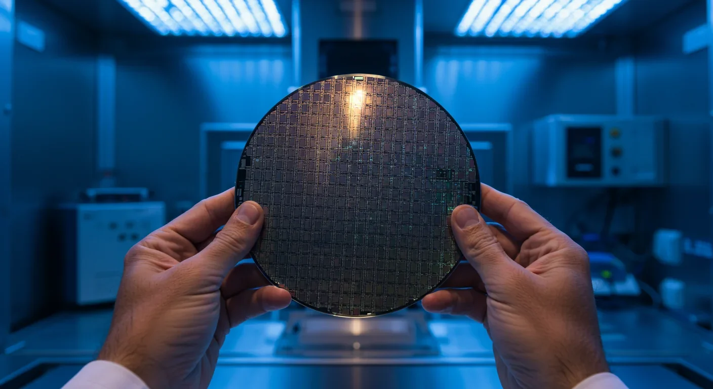
Silicon transistors have been shrinking for decades, but they're running out of room. When your chip channels get thinner than about a nanometer, quantum tunneling turns them into sieves - electrons leak through barriers that should stop them. Power consumption explodes. Performance collapses. We're hitting the hard wall where physics says "no further."
But while silicon approaches its twilight, carbon nanotubes are having their sunrise moment.
Moore's Law predicted that transistor density would double every two years, and for five decades it delivered. We went from room-sized computers to supercomputers in our pockets. But Moore's Law is reaching its physical limits, and the industry knows it. Below 5 nanometers, silicon transistors face insurmountable challenges: electron tunneling through thin gate oxides, short-channel effects where the gate loses control, leakage currents that waste power, and random variations from dopant placement.
These aren't engineering problems you can innovate around. They're fundamental physics saying you've reached the limit.
The semiconductor industry has squeezed remarkable performance from silicon by going vertical with 3D transistor architectures and using extreme ultraviolet lithography. But these are expensive workarounds, not solutions. Each new node costs more and delivers less improvement. The economic equation that powered the digital revolution is breaking down.
What happens when you can't make chips smaller, faster, and cheaper anymore? Either computing stagnates, or you change the material.
Carbon nanotubes are hollow cylinders of carbon atoms arranged in a hexagonal lattice, typically just 1-2 nanometers in diameter. That's roughly the width of a DNA helix. But what makes them revolutionary isn't their size - it's their electronic properties.
Unlike silicon, which conducts electricity through a three-dimensional bulk material, carbon nanotubes are effectively one-dimensional. Electrons travel along the tube's length in what physicists call "ballistic transport" - they move without scattering, almost like they're on rails. This means carbon nanotube transistors can be smaller, faster, and far more energy-efficient than silicon.
How much better? Recent demonstrations show carbon nanotube transistors achieving current densities more than four times higher than the best silicon devices of comparable size, operating at just 0.5 volts. A team at Tsinghua University built a prototype computing system that runs 119 times faster than conventional chips while using just 1/17th the energy.
These aren't marginal improvements. They're the kind of performance leaps that defined earlier eras of computing.
The theoretical advantages have been known since the 1990s. The problem was making carbon nanotube transistors work reliably at scale. For decades, the gap between laboratory demonstrations and commercial viability seemed unbridgeable.

Three fundamental challenges blocked carbon nanotube transistors from replacing silicon: purity, alignment, and doping.
Purity: When you grow carbon nanotubes, you get a mix of semiconducting tubes (which can switch on and off, making them useful for transistors) and metallic tubes (which conduct all the time, creating short circuits). Early processes produced roughly 30% semiconducting nanotubes. A single metallic tube among semiconducting ones would ruin an entire device.
Solution? Researchers at Peking University developed a selective catalytic growth method using single-atom iron seeds combined with specialized purification. They can now produce semiconducting nanotube purity above 99.99% - good enough for reliable circuits.
Alignment: Random tangles of carbon nanotubes don't make good transistors. You need them lined up in parallel arrays with precise spacing. The spacing - called pitch - has to be uniform across an entire wafer, or device characteristics vary wildly.
Teams at Stanford and MIT cracked this using optimized chemical vapor deposition on specially prepared substrates. They can grow aligned nanotube arrays with densities exceeding a billion tubes per square centimeter. Philip Wong at Stanford, who's been working on carbon nanotubes for two decades, says many of the fundamental problems have been solved.
Doping: Silicon transistors need both n-type (negative) and p-type (positive) regions to build complete circuits. Creating n-type carbon nanotube transistors was notoriously difficult because traditional doping disrupts the nanotube's perfect lattice structure.
The Stanford team developed a top-positioned doping method where dopants sit on top of the channel rather than embedded in it. This preserves the nanotube structure while enabling both n-type and p-type devices - essential for building full CMOS logic circuits.
Individually, each breakthrough was impressive. Together, they've transformed carbon nanotube transistors from a curiosity into a credible silicon successor.
Numbers tell the story. A research team demonstrated 10-nanometer channel length carbon nanotube transistors with on-currents exceeding 5 milliamps per micrometer - better than state-of-the-art 3-nanometer silicon chips. Another group achieved 400 GHz frequency response, surpassing silicon RF transistors by a factor of four.
But raw speed isn't the only metric. Energy efficiency matters more for most applications. Carbon nanotube circuits operate at lower voltages - often below 0.6 volts versus 0.9 volts or more for silicon. Since power consumption scales with the square of voltage, that's a massive reduction. One demonstration showed carbon nanotube logic circuits achieving a 60% reduction in energy-delay product compared to advanced 7-nanometer silicon nodes.
For mobile devices, that translates to longer battery life. For data centers consuming gigawatts of power, it means dramatically lower operating costs and carbon footprint. For AI accelerators processing trillions of operations, it enables capabilities that would melt silicon chips.
Perhaps most importantly, carbon nanotube transistors work at room temperature and don't require exotic materials or cryogenic cooling. They're a drop-in replacement for silicon in terms of basic operating environment, which matters enormously for commercial adoption.
The physics works. The performance is proven. Now it's an engineering and manufacturing problem.
Don't expect carbon nanotube processors in your next smartphone. The path from laboratory breakthrough to mass production typically takes a decade or more in the semiconductor industry.
The carbon nanotube market is projected to grow significantly through 2034, but most current applications focus on materials science - stronger composites, better batteries, enhanced coatings. Electronic applications are still emerging.
Several major players are positioning themselves: IBM has been investing in carbon nanotube research for over 15 years, Stanford's H-S Philip Wong leads academic efforts with industry partnerships including TSMC, MIT's Microsystems Technology Laboratories are developing manufacturing processes, and startups like SkyWater Technology and Carbon Solutions are commercializing production techniques.
The most likely adoption path starts with specialized applications where performance justifies higher costs: high-frequency RF circuits for 6G wireless communication, ultra-low-power sensors for IoT devices, AI accelerator chips for data centers, and space-qualified electronics where radiation hardness matters.
Consumer processors will come later. Think 2030-2035 for premium devices, 2035-2040 for mainstream adoption. That might sound distant, but semiconductor manufacturing cycles are measured in decades. Companies are making billion-dollar investments now for products they'll ship in 2028.

Even with recent breakthroughs, challenges remain. Achieving perfectly uniform nanotube pitch across 300mm wafers is still inconsistent. Process yields are improving but not yet at the 90%+ levels required for economic mass production. Contact resistance between metal electrodes and nanotubes adds unwanted power consumption.
Integration with existing fabrication facilities poses questions. Do you build entirely new fabs, or retrofit existing silicon lines? The answer affects economics dramatically. Stanford's approach of growing carbon nanotube circuits on top of completed silicon wafers - called back-end-of-line stacking - offers a hybrid path that could accelerate adoption.
Then there's the knowledge gap. The semiconductor industry employs hundreds of thousands of engineers who understand silicon intimately. Carbon nanotubes require different expertise. Training, documentation, and accumulated process wisdom need time to develop.
These are solvable problems, not fundamental barriers. But they explain why commercialization takes years even after scientific breakthroughs.
Technology this significant doesn't happen in a vacuum. The competition to lead next-generation computing has geopolitical dimensions.
China announced significant investments in carbon nanotube research as part of its semiconductor self-sufficiency push. Whether their claims of "silicon-free chips" represent actual breakthroughs or aspirational marketing remains debated, but the intent is clear.
The United States maintains research leadership through Stanford, MIT, and IBM, backed by DARPA funding. But translating research into manufacturing requires fabrication capacity, where Asia dominates. TSMC in Taiwan and Samsung in South Korea operate the world's most advanced fabs.
Europe is strengthening its position through university-industry collaborations and the EU's Chips Act, which allocates billions for semiconductor research and production capacity.
This isn't just about economics. Computing capability underpins everything from artificial intelligence to weapons systems. The nation that leads the post-silicon era gains strategic advantage across multiple domains.
Faster, more efficient computing doesn't just make existing applications better - it enables new ones.
Artificial intelligence today is constrained by power and heat. Training large language models requires datacenters consuming megawatts. Carbon nanotube processors could make AI inference cheap enough to run entirely on-device, eliminating privacy concerns and connectivity requirements.
Quantum computing needs classical control electronics that operate at cryogenic temperatures. Carbon nanotubes work fine when cold, unlike silicon which becomes less efficient. They could enable better qubit control and measurement.
Brain-computer interfaces require ultra-low-power processors small enough to implant. Carbon nanotube circuits could make neuroprosthetics practical for millions of people.
Edge computing in harsh environments - deep sea sensors, space missions, industrial monitoring - needs reliable electronics that handle radiation and temperature extremes. Carbon nanotubes are naturally radiation-hard and operate across wide temperature ranges.
These aren't incremental improvements to how we use computers today. They're new categories of applications that become possible when the fundamental constraints change.
Every major computing transition reshaped society. Mainframes created modern business. Microprocessors enabled personal computers, which democratized information. Mobile chips put supercomputers in everyone's pocket, which reconfigured how humans interact.
What happens when computing power improves by another 100x while energy consumption drops by 90%?
Ubiquitous AI becomes economically viable. Every device gets smart without cloud connectivity or privacy tradeoffs. Real-time language translation, personalized education, medical diagnostics at the point of care - capabilities we glimpse today become commonplace.
The environmental equation changes too. Data centers currently consume about 1% of global electricity. If AI continues scaling exponentially on silicon, that could reach 10% by 2030. Carbon nanotube processors could keep AI scaling while actually reducing energy consumption.
But there's a darker side. Compute-intensive surveillance becomes cheaper and more pervasive. Autonomous weapons get more capable. The digital divide between those with access to next-generation computing and those without could widen dramatically.
Technology doesn't determine outcomes - how we deploy it does.
Silicon gave us 50 years of exponential improvement. We built the modern world on that foundation. As silicon's era ends, the question isn't whether computing will continue advancing - it's what material enables the next chapter.
Carbon nanotubes are the leading candidate, but they're not the only one. Gallium nitride, two-dimensional antimony, silicon carbide, and other materials have advocates. Multiple technologies might coexist, each optimized for different applications.
What seems certain is that 2025-2030 represents an inflection point. The chips powering your devices in 2040 will likely use fundamentally different materials than today's processors. The manufacturing, performance characteristics, and enabled applications will be distinct.
We're watching one of those rare moments when the technological substrate of civilization shifts. Like the transition from vacuum tubes to transistors, or mechanical calculators to electronic computers, this isn't just about faster gadgets. It's about recalibrating what's possible.
The age of silicon revolutionized human society. The age of carbon nanotubes might do it again.
Your next computer might run on silicon. But your grandchildren's computers almost certainly won't. The question isn't if we'll move beyond silicon, but how quickly, and who will lead the transition.
The breakthrough that powers the next 50 years of computing is happening now, in labs at Stanford, in fabrication facilities in Taiwan, in research centers across China. The transistors are already working. The circuits are being proven. The manufacturing is scaling up.
By 2075, when someone asks what computers were like in the 2020s, "silicon-based" will be the defining descriptor - the same way we look back at vacuum tubes today. Quaint technology from an earlier era, replaced by something fundamentally better.
The future of computing fits in a hollow tube of carbon atoms one nanometer wide. And that future is closer than you think.

Saturn's moon Titan may harbour liquid water beneath its frozen crust, kept from freezing by ammonia acting as a natural antifreeze. New Cassini data suggests the interior could be slush with warm water pockets rather than a global ocean, and NASA's Dragonfly mission launching in 2028 aims to investigate whether this exotic environment could support life.

The cerebellum, long dismissed as merely a motor coordinator, forms dense circuits with the prefrontal cortex that shape cognition and emotion. Disruption of these pathways is now linked to schizophrenia, autism, and ADHD, opening new frontiers in diagnosis and non-invasive brain stimulation therapies.

Research shows the sharing economy often increases total resource consumption through the Jevons paradox and rebound effects. Ride-sharing adds billions of vehicle miles, co-working spaces use more energy per worker, and diffused responsibility erodes conservation behavior. Breaking the paradox requires congestion pricing, accountability design, and matching sharing models to appropriate resource types.

Illusory superiority causes most people to rate themselves above average in driving, intelligence, and ethics. This bias is rooted in metacognitive blind spots, shaped by culture, and carries real costs in healthcare, finance, and leadership. Structured feedback and institutional safeguards can help, but require ongoing effort.

Eastern skunk cabbage generates its own body heat through the alternative oxidase pathway, maintaining temperatures up to 35°C above freezing air and melting surrounding snow. This thermogenic ability, shared by roughly 90 plant species worldwide, reveals a level of metabolic sophistication that challenges assumptions about plant passivity.

America has 28 vacant homes for every homeless person, yet homelessness hit record highs in 2024. Speculative investment, geographic mismatches, and political barriers explain the paradox, while Finland and Vienna show that Housing First and social housing models can work when the political will exists.
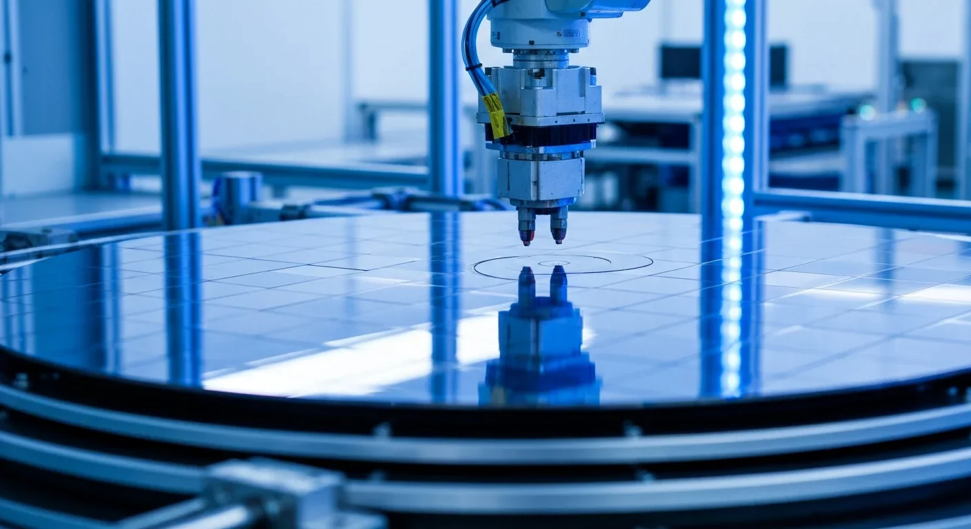
Wafer-on-wafer bonding fuses logic and memory silicon at the atomic level, delivering up to 100x interconnect density over traditional packaging. TSMC, Intel, and Samsung are racing to commercialize the technology as AI chips hit the memory bandwidth wall.

Loading featured articles...