Wafer-on-Wafer Bonding Breaks AI's Bandwidth Wall
Wafer-on-Wafer Bonding Breaks AI's Bandwidth Wall
Why Quantum Computers Need 1,000 Qubits for One
TPM 2.0 and Pluton: Hardware Root of Trust Explained
Why Quantum Computing Bet on One Qubit Design

P4 Programmable Switches Rewriting Networks at Tbps
Intel TSX Failed. Can ARM Fix Transactional Memory?
TL;DR: Through-silicon vias (TSVs) enable vertical chip stacking, solving the memory bandwidth crisis by creating direct vertical connections between dies. This technology powers AMD's 3D V-Cache, Intel's Foveros, and High Bandwidth Memory, delivering unprecedented performance for AI and HPC workloads.
What started as an experiment in Japanese research labs during the 1980s is now spreading worldwide. Through-silicon via (TSV) technology is fundamentally changing how we build computers, enabling chips to stack vertically like LEGO blocks. This breakthrough couldn't have come at a better time. Modern AI models and high-performance computing systems are hitting a wall: processors can crunch numbers faster than memory can deliver data. TSVs punch through this bottleneck by creating superhighways between stacked chips, slashing the distance data must travel from millimeters to micrometers.
For decades, chip designers made computers faster by shrinking transistors. The formula was simple: smaller transistors, higher clock speeds, better performance. But around the mid-2010s, that stopped working so well. Physics got in the way. Transistors got so small that heat became a nightmare, and making connections between chips using traditional wire bonds or flip-chip bumps started limiting everything.
Here's the problem: AI training workloads can require up to 1 TB/s of memory bandwidth, far beyond what traditional packaging can deliver. When your processor waits for data from memory, it's like having a Ferrari stuck in traffic. The engine's powerful but you're not going anywhere fast.
Traditional 2D packaging spreads chips horizontally across a circuit board or interposer. The connections travel along the surface, adding millimeters of wire length. Those millimeters translate to nanoseconds of delay and, more importantly, power consumption. Every picofarad of capacitance from those long wires drains your battery and slows your system.
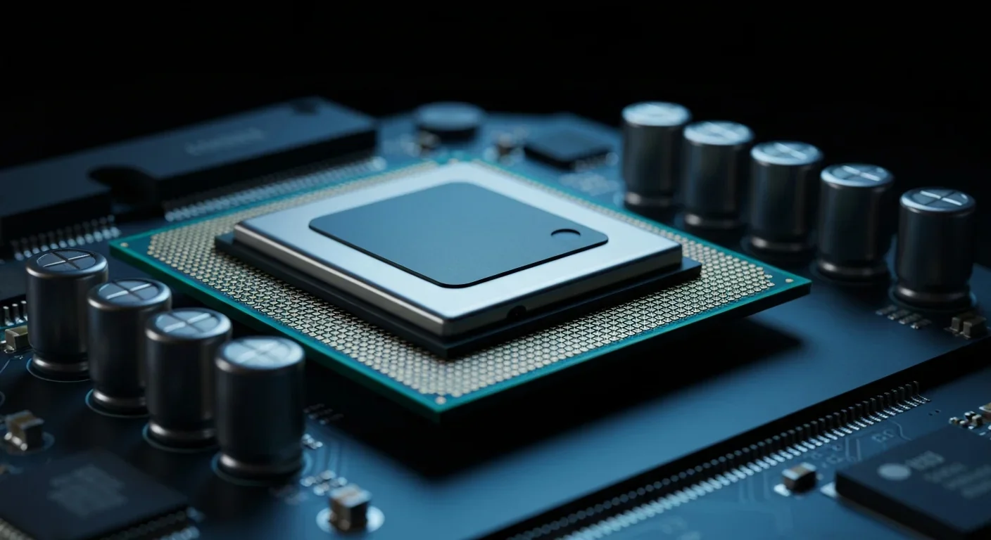
A through-silicon via is exactly what it sounds like: a vertical electrical connection that passes completely through a silicon wafer or die. Instead of routing signals around the edge of a chip or underneath it through a substrate, TSVs create direct vertical pathways.
Think of it like comparing the elevator in a skyscraper to walking down every hallway on every floor. The elevator (TSV) gets you there faster and with less effort. TSVs typically measure between 5 to 50 micrometers in diameter depending on the application, and they can be packed much more densely than traditional wire bonds or solder bumps.
TSVs reduce interconnect length from millimeters to micrometers, cutting latency and power consumption dramatically while enabling bandwidth densities impossible with traditional 2D packaging.
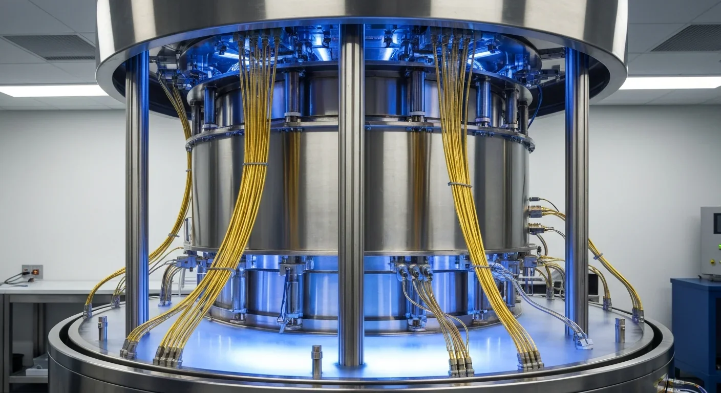
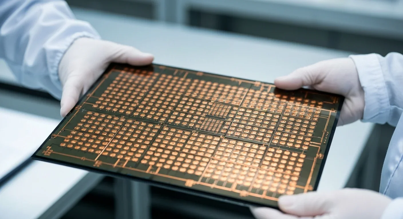
The manufacturing involves drilling or etching holes through the silicon, depositing an insulating layer to prevent electrical leakage, then filling the vias with copper or tungsten. It's a delicate process because silicon is brittle and the vias induce mechanical stress that can affect nearby transistors. But when done right, TSVs provide interconnect densities and bandwidths that were impossible just a decade ago.
Engineers developed three main approaches to manufacturing TSVs, each with distinct trade-offs. The choice depends on what you're building and what matters most: performance, cost, or flexibility.
Via-first creates TSVs before fabricating transistors. This approach integrates vias during the front-end-of-line (FEOL) process, which means the vias experience all the high-temperature steps of transistor manufacturing. That's tough on the copper filling but gives you the most design freedom. Via-first works well when you need high alignment accuracy for precision applications like high-performance computing.
Via-middle fabricates TSVs after transistors are patterned but before the metal interconnect layers. This is currently the most popular choice for advanced 3D ICs because it balances process complexity with interconnect density. The vias don't interfere with transistor formation, and you can still optimize the back-end metallization around them.
Via-last etches TSVs through the back of the wafer after all the front-side processing is complete. This approach minimizes thermal stress on transistors and allows you to use existing manufacturing processes with minimal modifications. However, via-last typically produces larger vias with lower density since you're drilling through from the back without the alignment precision of earlier integration.
Each method involves careful engineering of the via diameter, depth, aspect ratio, and pitch. Modern implementations are achieving pitches below 5 micrometers, enabling connection densities measured in thousands of I/Os per square millimeter.
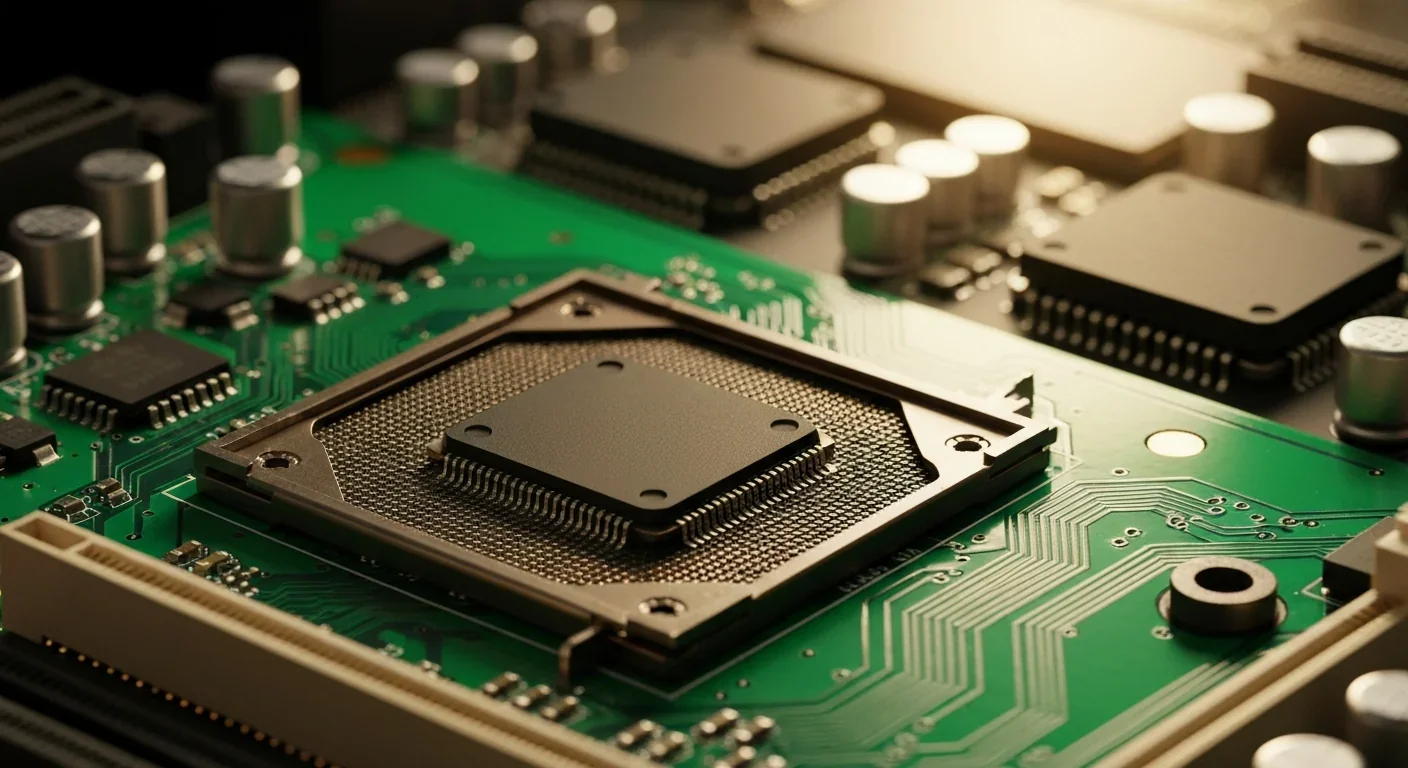
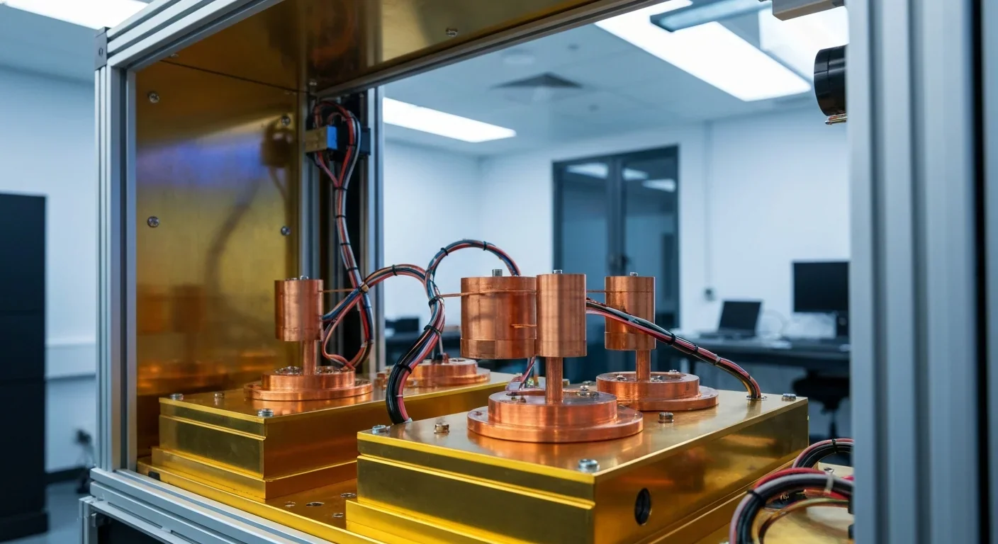
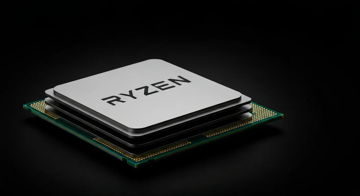
TSV technology moved from research labs to shipping products faster than almost anyone expected. The most visible success is AMD's 3D V-Cache, which stacks an additional 64 MB of L3 cache on top of processor cores using TSMC's SoIC hybrid bonding technology.
The manufacturing process thins the cache die to around 50 micrometers, creates TSVs through it, and bonds it directly to the core die using copper-to-copper connections with a 9 micrometer pitch. This gives AMD gaming CPUs like the Ryzen 9800X3D a significant performance advantage, with frame rates improving by over 20% in memory-intensive games compared to non-stacked equivalents.
"AMD's 3D V-Cache is a revolutionary cache technology that stacks additional L3 cache vertically on top of CPU cores."
- AMD official product description
Intel's response is Foveros Direct 3D, a packaging technology that enables active logic-on-logic stacking using face-to-face hybrid bonding. The latest variant, 18A-PT, will use bumpless copper-to-copper bonding with a pitch of less than 5 micrometers, a dramatic improvement over their initial 10 micrometer target. Foveros powered Intel's Ponte Vecchio GPU, which connects over 47 tiles using a combination of Foveros and EMIB technologies.
High Bandwidth Memory represents another massive TSV success story. HBM stacks multiple DRAM dies vertically using TSVs, creating a unified memory block sitting next to a GPU or accelerator on a silicon interposer. HBM delivers bandwidth exceeding 1 TB/s, which is exactly what modern AI training demands. NVIDIA's latest H100 and H200 GPUs rely on HBM3, and Samsung recently announced 12-layer HBM stacks using over 60,000 TSV holes while maintaining the same thickness as previous 8-layer designs.
TSVs solve the bandwidth problem but create new headaches. Thermal management tops the list. Stacking active dies vertically concentrates heat generation in a smaller volume. Thermal resistance in 3D stacked configurations can increase by 20 to 40 percent compared to planar designs, meaning the chips run hotter unless you implement sophisticated cooling.
Designers use several strategies to combat this. Thermal-aware floorplanning places hot functional blocks on different layers so they're not stacked directly on top of each other. Some designs position high-power cores on the top die where heat dissipation is easier, while low-power logic and memory sit beneath. Advanced implementations use dedicated thermal TSVs filled with materials that conduct heat better than the surrounding silicon.
Mechanical stress is another concern. TSVs induce thermomechanical stress that can alter transistor behavior. The copper filling expands and contracts differently than silicon during thermal cycling, potentially degrading performance or causing reliability issues. Via-first TSVs are particularly challenging because they experience all the high-temperature steps of device fabrication.
3D stacked chips can see thermal resistance increase by 20-40%, requiring sophisticated cooling strategies like thermal-aware floorplanning and dedicated thermal vias to prevent overheating.
Manufacturing yield adds cost pressure. Every additional process step is an opportunity for defects. Creating thousands of TSVs through a wafer, ensuring they're properly filled, and bonding dies together without misalignment requires extreme precision. Industry sources suggest that 3D stacked products currently cost 15 to 30 percent more than equivalent 2D implementations, though this premium is shrinking as volumes increase.
Design complexity shouldn't be underestimated either. Electronic design automation (EDA) tools must account for TSV effects during placement, routing, and verification. Power delivery networks become three-dimensional puzzles. Testing is harder because you can't easily probe internal layers once the stack is assembled. The entire design methodology shifts from flat 2D thinking to true 3D architecture.
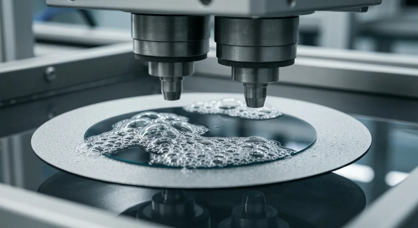
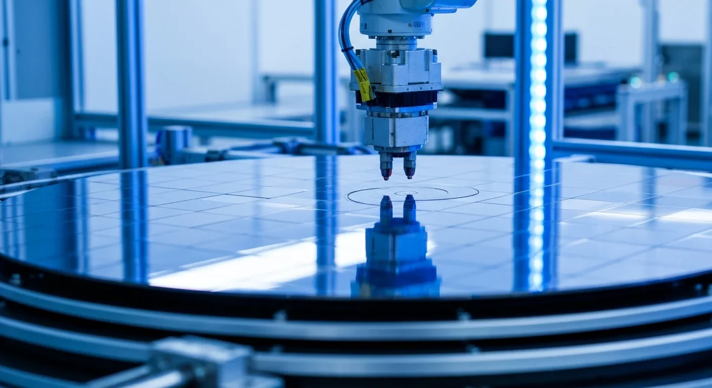
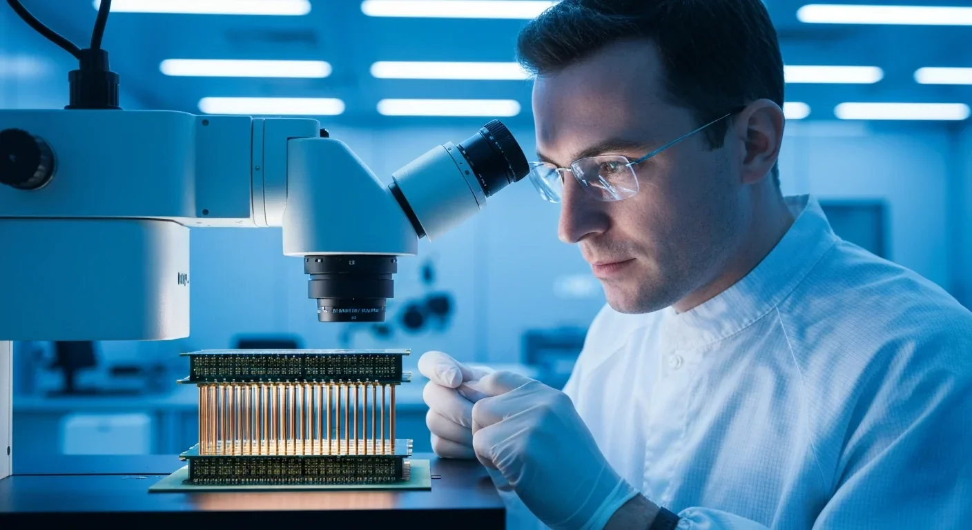
One aspect that doesn't get enough attention is cleaning the TSVs after etching. Residue from the etching process leaves polymer films and particles inside the vias. If you don't remove these completely, the copper filling won't adhere properly and you'll get electrical failures.
Megasonic cleaning uses high-frequency sound waves to create controlled cavitation in liquid, gently removing sidewall residue without damaging the silicon. Advanced systems use Space Alternated Phase Shift (SAPS) technology, which moves or tilts the megasonic transducer while the wafer rotates. This ensures uniform energy distribution across the wafer, even in deep TSVs with high aspect ratios. SEM analysis shows that SAPS megasonic cleaning completely removes fluoropolymer residue that would otherwise degrade TSV reliability.
The TSV technology market was valued at approximately $3.5 billion in 2023 and is projected to reach nearly $10.4 billion by 2032, expanding at a 12.7% compound annual growth rate. Another forecast puts the broader 3D IC market at over $15 billion by 2028. These aren't just numbers on a slide; they represent massive capital investments in fabs, equipment, and talent.
Asia Pacific dominates the landscape, accounting for roughly 45% of the global TSV market share in 2023 and expected to grow at 13.5% CAGR. Taiwan's TSMC leads in advanced packaging through CoWoS and SoIC technologies. Samsung in South Korea is pushing HBM and 3D DRAM aggressively. China is investing heavily despite export controls that limit access to cutting-edge lithography equipment.
The United States is responding. Intel has begun upgrading its New Mexico facilities to support advanced packaging, with Fab 9 and Fab 11x in Rio Rancho now mass-producing Intel's 3D packaging technologies. Intel is also making Foveros available to foundry customers, and companies like Apple and Qualcomm are reportedly seeking talent with EMIB expertise, signaling growing interest in Intel's advanced packaging ecosystem.
"Intel's EMIB and Foveros technologies are seeing growing interest, with Apple and Qualcomm posting job openings seeking talent experienced in its EMIB packaging."
- TrendForce News
This geographic distribution matters for supply chain resilience and geopolitical strategy. When most advanced packaging capability sits in a single region, it creates vulnerability. The push to diversify manufacturing locations reflects lessons learned from recent chip shortages and growing tensions over semiconductor technology access.
TSV-enabled 3D stacking isn't just an incremental improvement. It fundamentally changes what's architecturally possible. When you can stack compute, memory, and specialized accelerators vertically with thousands of interconnects per square millimeter, you can design systems that were physically impossible before.
Chiplet architectures become more practical. Instead of fabricating a monolithic 500mm² die with terrible yield, you can build multiple smaller chiplets on optimal process nodes and stack or place them together. Your high-performance cores might use a cutting-edge 3nm process, while I/O and analog functions use a mature 22nm node where they're cheaper to produce. Heterogeneous integration lets you mix different technologies that couldn't be fabricated on the same wafer.
Near-memory computing becomes realistic at scale. Traditionally, memory sits far from the processor, separated by a bus that creates latency and power overhead. With 3D stacking, you can place memory dies directly above or below compute logic, enabling processing-in-memory architectures that dramatically reduce data movement. For AI inference workloads where the same weights are used repeatedly, this could cut energy consumption by an order of magnitude.
Optical interconnects might finally reach the chip level. Research teams are exploring photonic integration where optical components are stacked above electronic logic using TSVs for power and control signals. Light travels faster than electrons and doesn't suffer from the same RC delay limitations. If this matures, we could see chip-to-chip communication at terabits per second with minimal power draw.
There's a talent shortage brewing. Designing 3D stacked systems requires expertise that crosses traditional boundaries: you need to understand advanced packaging, thermal management, power delivery, signal integrity, and manufacturing constraints simultaneously. Universities are just starting to update curricula. Companies are competing aggressively for engineers with 3D IC experience.
The job postings tell the story. Apple and Qualcomm are looking for people who understand Intel's EMIB technology, even though they've historically relied on TSMC for packaging. That cross-pollination of expertise suggests the industry recognizes that 3D integration is becoming table stakes, not a differentiator.
Tool vendors are scrambling to keep up. EDA tools need to handle 3D thermal simulation, power delivery analysis across multiple dies, and electromagnetic effects that traditional 2D tools ignore. Testing equipment must verify stacked dies without being able to physically probe every layer. The entire semiconductor ecosystem is transforming.
The next decade will see 3D chip stacking move from high-end specialty products to mainstream computing. Mobile processors will stack compute, graphics, and memory to save space and power. Data center accelerators will stack logic, HBM, and potentially photonics in single packages optimized for specific AI workloads. Even commodity DRAM might eventually adopt 3D architectures to continue scaling capacity.
The economics are starting to make sense. While 3D stacking currently adds 15 to 30 percent cost premium, that's dropping as yields improve and volumes increase. When you account for the system-level benefits - reduced PCB complexity, smaller form factors, lower power consumption - the total cost of ownership often favors 3D solutions already.
As manufacturing volumes increase and yields improve, the cost premium for 3D stacked chips is shrinking rapidly, making vertical integration economically viable for mainstream computing applications within this decade.
TSVs represent a rare technology that solves multiple problems simultaneously. They address the memory bandwidth bottleneck. They enable continued performance scaling as transistor shrinking slows. They allow heterogeneous integration of different technologies. And they do this while potentially reducing overall system power consumption, which matters tremendously for everything from smartphones to data centers.
The era of flat chips is ending. The computers of tomorrow will grow vertically, stacking functionality layer by layer with TSVs threading through them like neural pathways. What started in those Japanese labs four decades ago is finally becoming the foundation of how we build high-performance computing systems. The memory bandwidth crisis that threatened to stall AI and HPC progress has met its match in a deceptively simple idea: when you can't go wider, go up.

Saturn's moon Titan may harbour liquid water beneath its frozen crust, kept from freezing by ammonia acting as a natural antifreeze. New Cassini data suggests the interior could be slush with warm water pockets rather than a global ocean, and NASA's Dragonfly mission launching in 2028 aims to investigate whether this exotic environment could support life.

The cerebellum, long dismissed as merely a motor coordinator, forms dense circuits with the prefrontal cortex that shape cognition and emotion. Disruption of these pathways is now linked to schizophrenia, autism, and ADHD, opening new frontiers in diagnosis and non-invasive brain stimulation therapies.

Research shows the sharing economy often increases total resource consumption through the Jevons paradox and rebound effects. Ride-sharing adds billions of vehicle miles, co-working spaces use more energy per worker, and diffused responsibility erodes conservation behavior. Breaking the paradox requires congestion pricing, accountability design, and matching sharing models to appropriate resource types.

Illusory superiority causes most people to rate themselves above average in driving, intelligence, and ethics. This bias is rooted in metacognitive blind spots, shaped by culture, and carries real costs in healthcare, finance, and leadership. Structured feedback and institutional safeguards can help, but require ongoing effort.

Eastern skunk cabbage generates its own body heat through the alternative oxidase pathway, maintaining temperatures up to 35°C above freezing air and melting surrounding snow. This thermogenic ability, shared by roughly 90 plant species worldwide, reveals a level of metabolic sophistication that challenges assumptions about plant passivity.

America has 28 vacant homes for every homeless person, yet homelessness hit record highs in 2024. Speculative investment, geographic mismatches, and political barriers explain the paradox, while Finland and Vienna show that Housing First and social housing models can work when the political will exists.
Wafer-on-wafer bonding fuses logic and memory silicon at the atomic level, delivering up to 100x interconnect density over traditional packaging. TSMC, Intel, and Samsung are racing to commercialize the technology as AI chips hit the memory bandwidth wall.

Loading featured articles...