Wafer-on-Wafer Bonding Breaks AI's Bandwidth Wall
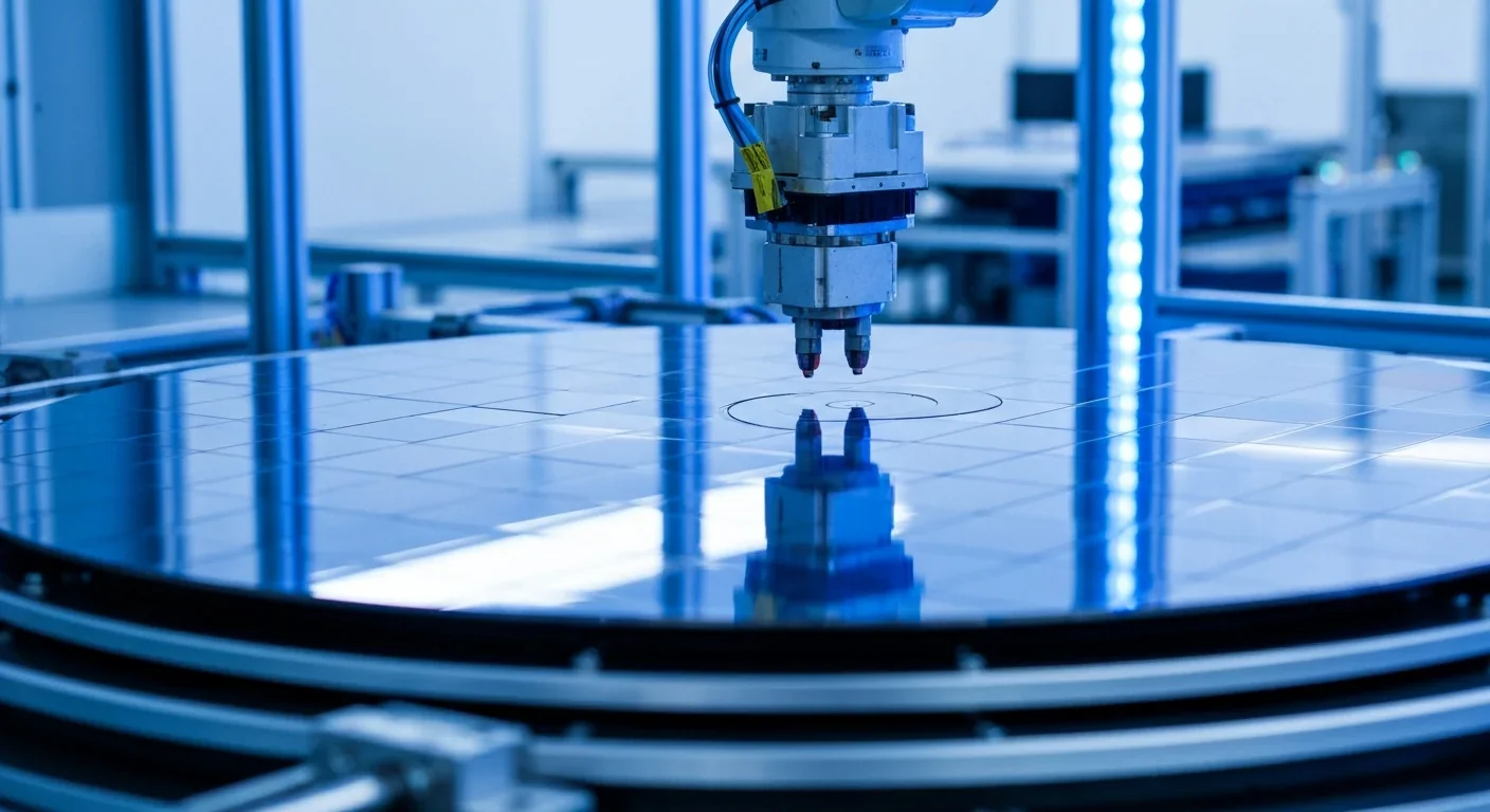
Wafer-on-Wafer Bonding Breaks AI's Bandwidth Wall
Why Quantum Computers Need 1,000 Qubits for One
TPM 2.0 and Pluton: Hardware Root of Trust Explained
Why Quantum Computing Bet on One Qubit Design
P4 Programmable Switches Rewriting Networks at Tbps
Intel TSX Failed. Can ARM Fix Transactional Memory?
TL;DR: Google's seven TPU generations achieved 128x performance improvement through architectural innovation, vertical integration, and specialized AI silicon design - challenging NVIDIA's GPU dominance while powering breakthroughs from AlphaGo to Gemini.
In March 2016, a 31-year-old South Korean chess prodigy sat across from a machine. Lee Sedol, one of humanity's greatest Go players, faced Google's AlphaGo in a five-game match that captivated 280 million viewers worldwide. Behind AlphaGo's mind sat something the public hadn't seen: a custom chip Google had been developing in secret since 2013. That chip, the first Tensor Processing Unit, would power not just AlphaGo's historic victory but an entire generation of AI breakthroughs that followed.
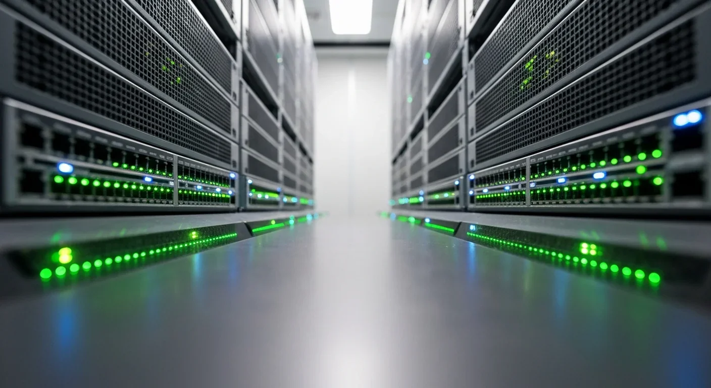
Seven years and seven chip generations later, those same TPUs now train models like Gemini and process billions of searches, translations, and image recognitions daily. What started as a desperate measure to avoid doubling Google's data centers has become the company's most formidable competitive advantage against NVIDIA's GPU dominance. This is the story of how Google achieved something Silicon Valley said was impossible: doubling AI performance with each generation while the rest of the industry struggled to keep pace with Moore's Law.
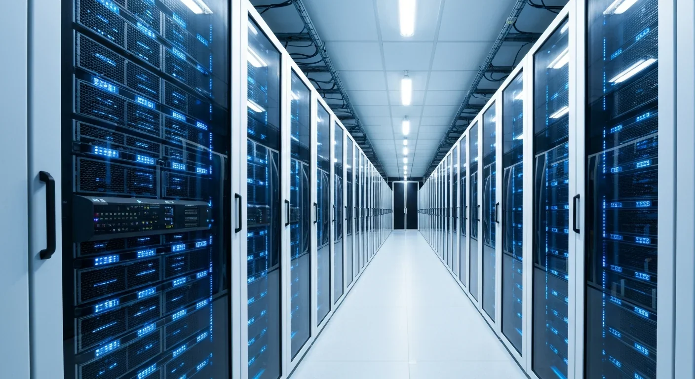
In 2013, Google engineers faced a terrifying projection. If voice search took off and people started using it just three minutes per day, the company would need to double its entire data center infrastructure - thousands of servers, millions of GPUs, hundreds of megawatts of power. The cost would be astronomical. The timeline? Impossible.
The team had 15 months to solve a problem that traditionally took semiconductor companies three to five years. They couldn't wait for NVIDIA's next GPU generation. They couldn't even wait for the traditional chip design process. So they did something radical: they built a chip that could only do one thing, but could do it better than anything else on Earth - matrix multiplication for neural networks.
Google's first TPU was built in just 15 months to avoid doubling their entire data center infrastructure - a timeline that would typically take semiconductor companies 3-5 years.
That first TPU wasn't pretty. Built on a relatively ancient 28-nanometer process when competitors were moving to 14nm, it looked dated before it even launched. But TPUv1's 256×256 systolic array of 8-bit integer multiply-accumulate units delivered something unprecedented: 92 teraops per second while consuming just 28 to 40 watts. That was 15 to 30 times faster than contemporary CPUs and GPUs for inference tasks, with 30 to 80 times better performance per watt.
The secret wasn't the process node. It was specialization so extreme it bordered on reckless. While GPUs carried the baggage of rendering graphics - texture mapping, rasterization, all the complexity of drawing pixels on screens - TPUs stripped everything away except the mathematical core of neural networks. No graphics. No general-purpose computing. Just relentless, efficient matrix math.
AlphaGo's victory proved TPUv1 could handle inference, feeding data through trained models to make predictions. But by 2017, Google faced a different challenge: training those models in the first place required vastly more computational power and a completely different kind of math.
TPUv2, released in May 2017, marked Google's bet that custom silicon could dominate training workloads too. The architecture shift was fundamental. Instead of integer-only computation, TPUv2 introduced support for bfloat16 - a floating-point format that preserved the range of 32-bit floats while cutting the bits in half. It featured dual 128×128 multiply-accumulate units per core, 16GB of High Bandwidth Memory delivering 600 GB/s, and perhaps most critically, a 2-D torus interconnect that let chips talk to each other at unprecedented speeds.

This wasn't just an evolution. It was a complete architectural reimagining. Where TPUv1 lived in isolation, crunching through inference requests one at a time, TPUv2 pods networked 256 chips together into supercomputers delivering 11.5 petaflops of computing power. That's more computing muscle than the world's fastest supercomputer from just a decade earlier, purpose-built for a single task: training neural networks.
The doublings Google claimed weren't just about raw speed. They came from rethinking the entire stack. The Inter-Chip Interconnect used a weight-stationary dataflow that minimized the most expensive operation in computing - moving data. By keeping weights in place and streaming activations through the systolic array, TPUs maximized data reuse and slashed memory traffic. In AI computing, the bottleneck isn't calculation anymore. It's moving numbers around.
"Specialization of the caches and register files, which traditionally consume the majority of processor die energy, is a critical design choice for AI accelerators. By concentrating on data-movement patterns, TPUs achieve far higher FLOPs per watt than general-purpose GPUs."
- ASCII News Technical Analysis
When Google announced TPUv3 in 2018, the company did something unprecedented for machine learning chips: it added liquid cooling. Not because it wanted to, but because it had to.
TPUv3 delivered 420 teraflops per chip - more than doubling TPUv2's performance. But that power came at a literal cost: heat. So much heat that air cooling couldn't handle it. Google had to engineer custom water-cooling systems that could be deployed across entire data center racks, a logistical nightmare that would have killed most chip projects.
Why push so hard? Because by 2018, the AI race had intensified. DeepMind was training increasingly sophisticated models. Google Brain was pushing the boundaries of natural language processing. BERT, one of the most influential language models before the GPT era, would train on TPUv3 pods. The models were getting exponentially larger, and the only way to keep training times reasonable was to throw more computational power at the problem.
TPUv3 expanded pods to 1,024 chips, quadrupling the cluster size from TPUv2. These weren't incremental improvements - they were the kind of scaling jumps that define technological eras. Each pod delivered over 100 petaflops of computing power, enough to train models that would have been impossible just two years earlier.
But liquid cooling was a warning sign. Google was hitting physical limits. You can only push silicon so far before thermodynamics wins. The next generation would need to be smarter, not just faster.
May 2021 brought TPUv4, and with it, a breakthrough that semiconductor experts had been predicting for decades but struggling to commercialize: optical circuit switching at data center scale.
The problem TPUv4 solved wasn't just about individual chip performance. It was about connecting 4,096 chips into a single coherent supercomputer without the interconnect becoming a bottleneck. Traditional electrical switches couldn't handle the bandwidth. Google's solution: 13,824 optical ports across 48 optical circuit switching units, managing photons instead of electrons to wire the entire pod together.
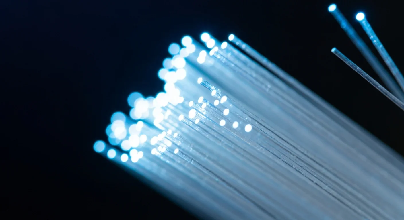
The impact was staggering. Optical switching eliminated packet-switching latency, enabling sub-10-nanosecond reconfiguration of the network topology. That meant TPU clusters could dynamically reshape themselves in real-time, adapting to different workload patterns. The interconnect became 10 times faster than TPUv3's already impressive network.
Google also introduced SparseCore accelerators - specialized units designed to handle the sparse matrices common in embeddings for recommendation systems and language models. While the main systolic arrays churned through dense matrix multiplication, SparseCores handled the irregular, patchy data structures that conventional accelerators struggled with.
TPUv4 represented a 2x performance leap over TPUv3, but more importantly, it showed that Google's vertical integration strategy - controlling silicon, networking, compilers, and frameworks - could deliver architectural innovations that competitors couldn't match. NVIDIA had faster individual GPUs, but Google had faster systems.
In December 2023, Google revealed something that sounded like science fiction: TPUv5's physical layout was designed by artificial intelligence.
Using deep reinforcement learning, Google's engineers let algorithms optimize the placement of billions of transistors on the chip's die. Where human designers might take months to lay out a chip, considering thousands of variables affecting signal timing, power consumption, and heat distribution, AI systems could explore millions of design variations in days.
TPUv5's chip layout was designed using deep reinforcement learning, allowing AI to optimize transistor placement by exploring millions of design variations - a process that would take human designers months.
The results spoke for themselves. TPUv5 delivered nearly double TPUv4's performance while competing head-to-head with NVIDIA's H100 - widely considered the most powerful AI training GPU available. But the real innovation wasn't just the performance numbers. It was proving that AI could design better AI hardware, creating a feedback loop that could accelerate future generations.
TPUv5 introduced several variants optimized for different workloads. The v5p (performance) version packed 459 TFLOPs and 96GB of memory per chip, while the v5e (efficiency) version prioritized cost-effectiveness for inference and lighter training tasks. This segmentation reflected AI workload reality: not every task needs maximum power. Sometimes efficiency and cost matter more than raw performance.
When Google announced TPUv6 Trillium, silicon experts did a double-take. The chip was manufactured on the same N5 process node as TPUv5p - no Moore's Law improvements, no smaller transistors - yet delivered a 2x increase in peak theoretical FLOPs with significantly less power.
How? Google quadrupled the size of each systolic array from 128×128 tiles to 256×256 tiles. That's four times as many multiply-accumulate units cranking through matrix operations simultaneously. But making that work required rethinking memory bandwidth, interconnect topology, and power delivery. Trillium showed that architectural innovation could still deliver performance doublings even when process technology stalled.
A former Google Cloud employee put it bluntly: "TPU v6 is 60-65% more efficient than GPUs, prior generations 40-45%." That efficiency gap represented billions of dollars in data center operating costs and a massive environmental advantage.
Trillium also demonstrated Google's manufacturing strategy. By partnering with Broadcom for backend manufacturing while controlling frontend design, Google could iterate faster than competitors dependent on external chip manufacturers. When TSMC's leading-edge nodes hit capacity constraints, Google had alternative paths to production.
The latest salvo in the AI accelerator wars came with TPUv7 Ironwood, Google's most aggressive play yet. The specifications read like a direct challenge to NVIDIA's Blackwell architecture: 4,614 TFLOPs of bfloat16 performance, 192GB of HBM3E memory, and 7,370 GB/s of memory bandwidth.
Those numbers nearly close the gap with NVIDIA's flagship GPUs, though Ironwood shipped about a year after Blackwell's announcement. But Google's pitch isn't just about matching specs. It's about total cost of ownership. According to industry analysis, the all-in TCO per Ironwood chip for the full 3D Torus configuration is roughly 44% lower than the TCO of a GB200 server.
That cost advantage comes from vertical integration. Google controls the entire stack - silicon design, system architecture, network topology, compiler toolchain, and software frameworks. When you buy TPU cloud instances, you're not just renting chips. You're accessing an entire co-designed ecosystem optimized for AI workloads.
The network architecture particularly stands out. TPU's Inter-Chip Interconnect delivers up to 100 Gbps per link with 1.2 TB/s aggregate bandwidth (compared to NVIDIA NVLink's 1.8 TB/s), enabling massive cluster sizes without interconnect bottlenecks. The 3D torus topology means each chip has direct paths to six neighbors, creating a hypercube-like network that keeps latency predictable even at 4,096-chip scale.
Ironwood also powers Google's Gemini models, showcasing the virtuous cycle between Google's AI research and hardware development. Each generation of models informs the next generation of chips, which enables the next generation of models. That tight feedback loop is nearly impossible for competitors to replicate.
"The more TPU you buy, the more NVIDIA GPU capex you save!"
- SemiAnalysis Newsletter on TPU competitive positioning
Here's what the raw performance numbers don't tell you: TPU vs. GPU debates miss the point. The real competition isn't hardware specs. It's ecosystems.
NVIDIA has CUDA - arguably the most successful software platform in computing history. Millions of developers know CUDA. Countless AI frameworks, libraries, and tools assume CUDA. Universities teach CUDA. That network effect creates enormous switching costs, even when alternatives offer better price-performance.
Google counters with TensorFlow, JAX, and XLA (Accelerated Linear Algebra) compiler technology. These frameworks abstract away hardware details, letting developers write model code once and run it on TPUs, GPUs, or CPUs. But adoption has been slower than Google hoped, particularly outside Google's own projects.
A former Google Cloud employee explained the adoption challenge: "The main problem for TPUs adoption is the ecosystem. NVIDIA's CUDA is engraved... organizations avoid TPUs despite performance benefits" because data transfer costs between clouds and lack of multi-cloud flexibility create vendor lock-in concerns.
That's changing, though. Google has aggressively expanded PyTorch support on TPUs through the PyTorch/XLA bridge, letting developers use the most popular deep learning framework while leveraging TPU performance. Major AI labs like Anthropic have signed massive TPU deals, including a reported 1MW+ buildout and 400,000+ TPUv7 chip order.
The ecosystem battle also plays out in pricing. Cloud customers report significant cost advantages. As one AlphaSense client noted: "If I were to use eight H100s versus using one v5e pod, I would spend a lot less money on one v5e pod." When training runs cost millions of dollars, those savings matter enormously.
Google's claim of doubling performance each generation deserves scrutiny. What exactly doubled?
The answer varies by generation and metric. TPUv1 to TPUv2 wasn't a straightforward doubling - it was a categorical shift from integer inference to floating-point training. Comparing them directly is like comparing a calculator to a supercomputer. They solve different problems.
TPUv2 to TPUv3 achieved roughly 2x peak FLOPs (180 to 420 TFLOPs per chip) through a combination of architectural tweaks, modest process improvements, and higher power budgets enabled by liquid cooling. The pod-level scaling from 256 to 1,024 chips delivered even larger total throughput jumps.
TPUv3 to TPUv4 doubled performance again, but the innovation was predominantly in the interconnect. Optical circuit switching and the 3D torus network enabled larger, more efficient clusters. Individual chip gains were more modest, but system-level performance exploded.
TPUv4 to TPUv5 achieved ~2x improvements partly through AI-driven chip design, partly through manufacturing refinements, and partly through continued scaling. The reinforcement learning approach to layout optimization found efficiencies human designers missed, squeezing more performance from similar silicon budgets.
TPUv5 to TPUv6 delivered perhaps the most impressive doubling: same process node, 2x performance. That came entirely from architectural innovation - quadrupling the systolic array size and rebalancing the chip's memory hierarchy and power delivery to support it. It proved that clever engineering could still matter more than Moore's Law.
Seven generations of ~2x improvements compound to roughly 128x total performance increase from TPUv1 to TPUv7 - and the strategies for achieving each doubling were completely different.
The pattern reveals Google's strategy: attack performance from every angle simultaneously. Shrink the process node when possible. Improve the architecture always. Scale the interconnect aggressively. Co-design the software stack. Iterate faster than competitors. The doublings aren't sleight of hand - they're the result of vertical integration and sustained engineering excellence.
Beyond Google's data centers, TPUs have fundamentally shaped AI development in ways that aren't always obvious.
First, they proved that domain-specific architectures could compete with general-purpose GPUs, spurring an explosion of AI accelerator startups. Companies like Cerebras, Graphcore, and SambaNova emerged with their own novel architectures, attracting billions in venture funding. Even NVIDIA responded by making its GPUs more AI-specific, introducing Tensor Cores and other specialized units.
Second, TPUs demonstrated that vertical integration - owning the full stack from silicon to software - could deliver competitive advantages even in mature markets. Apple's M-series chips and Amazon's Graviton processors followed similar playbooks, building custom silicon tightly integrated with their ecosystems.
Third, the TPU program showed that non-traditional chip companies could execute complex semiconductor projects. Google, a software and services company, shipped seven generations of leading-edge AI chips in under a decade. That inspired other tech giants to pursue custom silicon rather than relying solely on merchant chip vendors.
Fourth, TPUs accelerated specific AI breakthroughs that might not have been economically feasible on GPUs. AlphaGo, BERT, and Gemini all benefited from TPU performance and efficiency. Would these models have been trained anyway? Probably. But TPUs made them cheaper and faster, lowering the barrier to entry for large-scale AI research.
Finally, TPUs forced a broader conversation about energy efficiency in AI. As models ballooned from millions to billions to trillions of parameters, training costs spiraled into the millions of dollars - and megawatt-hours of electricity. TPUs' performance-per-watt advantage (30-80x better than early GPUs) made certain research directions viable that would have been economically or environmentally prohibitive otherwise.
Seven generations of ~2x improvements compound to roughly 128x total performance increase from TPUv1 to TPUv7. That's an extraordinary achievement, but it raises an obvious question: can it continue?
Physics imposes hard limits. You can only shrink transistors so far before quantum effects interfere. You can only clock chips so fast before heat becomes unmanageable. You can only pack components so densely before power delivery fails. Google has already hit some of these walls - hence the liquid cooling in TPUv3 and the focus on architectural innovation in TPUv6.
The next doublings will likely come from increasingly creative sources. Sparsity is one promising direction - most neural network matrices contain many zeros that don't need computation. SparseCore accelerators in TPUv4 previewed this approach. Future generations might aggressively prune unnecessary calculations, delivering effective performance gains without actually computing faster.
Memory technology matters enormously. High Bandwidth Memory has been critical to TPU performance, but it's also expensive and power-hungry. New memory technologies like MRAM or photonic memory could change the economics. So could near-memory computing that processes data right where it's stored, avoiding expensive data movement.
Network architectures will continue evolving. Optical interconnects are just the beginning. Silicon photonics might eventually bring optical signaling onto the chip itself, shattering bandwidth limits. Three-dimensional chip stacking could create short vertical connections between compute layers, reducing latency dramatically.
AI-designed AI chips represent perhaps the most intriguing path forward. TPUv5's reinforcement learning approach to layout optimization was a first step. Future generations might use AI to design entire architectures, not just optimize layouts. Imagine chips that evolve through machine learning, testing millions of architectural variations in simulation before a single wafer is manufactured.
And there's the software stack. Better compilers, smarter parallelization strategies, and improved model architectures can all deliver effective performance improvements without touching hardware. Google's XLA compiler has already wrung significant gains by optimizing operations specifically for TPU execution patterns. Future compiler improvements might matter as much as hardware generations.
If you're not building AI infrastructure at Google scale, why should you care about TPU evolution?
Because the innovations pioneered in TPUs eventually trickle down to everything. The bfloat16 format introduced in TPUv2 is now widely adopted across the AI industry, enabling more efficient training on diverse hardware. Systolic array architectures have influenced designs from Apple to startups. Optical circuit switching, once exotic, is becoming mainstream in data centers.
For developers, TPUs represent a viable alternative to NVIDIA's GPU monopoly - important for both cost and supply chain resilience. When GPU shortages constrained AI development in recent years, TPUs provided an escape valve. That competition benefits everyone by keeping prices in check and spurring innovation.
For organizations deploying AI, understanding the architectural trade-offs between TPUs and GPUs matters increasingly. Inference workloads might run far more efficiently on specialized hardware. Training certain model architectures could be dramatically cheaper on TPUs. The era of "just throw it on GPUs" is ending as options proliferate.
For society more broadly, the energy efficiency story matters enormously. If AI becomes as ubiquitous as experts predict - powering search, translation, recommendations, autonomous systems, and countless applications we haven't imagined - the energy cost could be staggering. Hardware innovations that deliver 60-65% efficiency gains over alternatives could be the difference between sustainable AI and environmental catastrophe.
The irony of TPUs is that their biggest impact might be the one we notice least. These chips power technologies so deeply embedded in daily life that they're invisible - Google Search understanding complex queries, Google Translate bridging languages in real-time, Google Photos recognizing faces and objects, Google Maps predicting traffic patterns.
Hundreds of millions of people interact with TPU-powered AI every day without knowing these chips exist. That's both TPUs' greatest success and their obscurity curse. NVIDIA GPUs get the headlines because developers buy them directly, stick them in visible servers, and talk about them constantly. TPUs hide behind APIs, working quietly in Google's data centers.
But make no mistake: the race between TPUs and GPUs will shape computing's next decade. Google has demonstrated that vertical integration, architectural creativity, and relentless iteration can challenge even the most entrenched incumbents. Seven generations in seven years, each roughly doubling performance. That's a pace most thought unsustainable.
The question isn't whether Google can keep doubling performance. The question is what becomes possible when AI compute continues getting exponentially cheaper and more efficient. Models that cost $100 million to train today might cost $1 million in a few years. Capabilities that require warehouse-sized data centers might fit on edge devices. Applications we haven't imagined might become trivial.
That's the real story of TPUs - not the technical specifications or competitive posturing, but the quiet acceleration of what's computationally possible. Seven generations have transformed AI from a research curiosity to society's next platform shift. What the next seven generations enable could reshape civilization itself.
And it all started because Google didn't want to double its data centers.

Saturn's moon Titan may harbour liquid water beneath its frozen crust, kept from freezing by ammonia acting as a natural antifreeze. New Cassini data suggests the interior could be slush with warm water pockets rather than a global ocean, and NASA's Dragonfly mission launching in 2028 aims to investigate whether this exotic environment could support life.
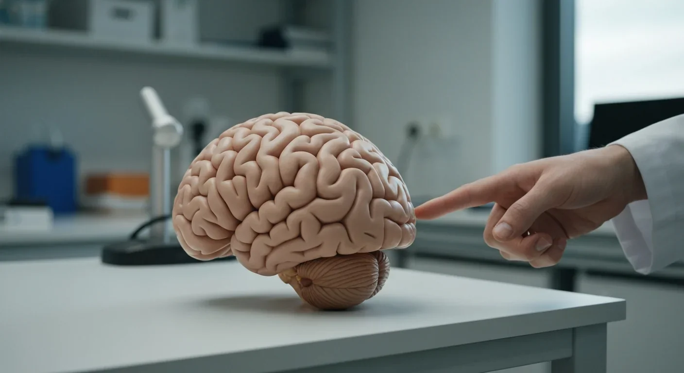
The cerebellum, long dismissed as merely a motor coordinator, forms dense circuits with the prefrontal cortex that shape cognition and emotion. Disruption of these pathways is now linked to schizophrenia, autism, and ADHD, opening new frontiers in diagnosis and non-invasive brain stimulation therapies.
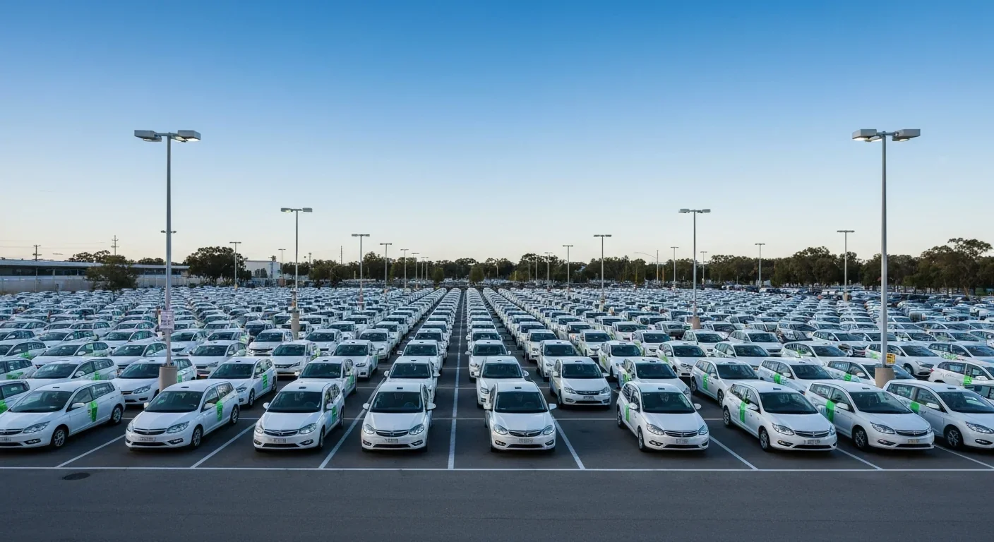
Research shows the sharing economy often increases total resource consumption through the Jevons paradox and rebound effects. Ride-sharing adds billions of vehicle miles, co-working spaces use more energy per worker, and diffused responsibility erodes conservation behavior. Breaking the paradox requires congestion pricing, accountability design, and matching sharing models to appropriate resource types.

Illusory superiority causes most people to rate themselves above average in driving, intelligence, and ethics. This bias is rooted in metacognitive blind spots, shaped by culture, and carries real costs in healthcare, finance, and leadership. Structured feedback and institutional safeguards can help, but require ongoing effort.

Eastern skunk cabbage generates its own body heat through the alternative oxidase pathway, maintaining temperatures up to 35°C above freezing air and melting surrounding snow. This thermogenic ability, shared by roughly 90 plant species worldwide, reveals a level of metabolic sophistication that challenges assumptions about plant passivity.

America has 28 vacant homes for every homeless person, yet homelessness hit record highs in 2024. Speculative investment, geographic mismatches, and political barriers explain the paradox, while Finland and Vienna show that Housing First and social housing models can work when the political will exists.
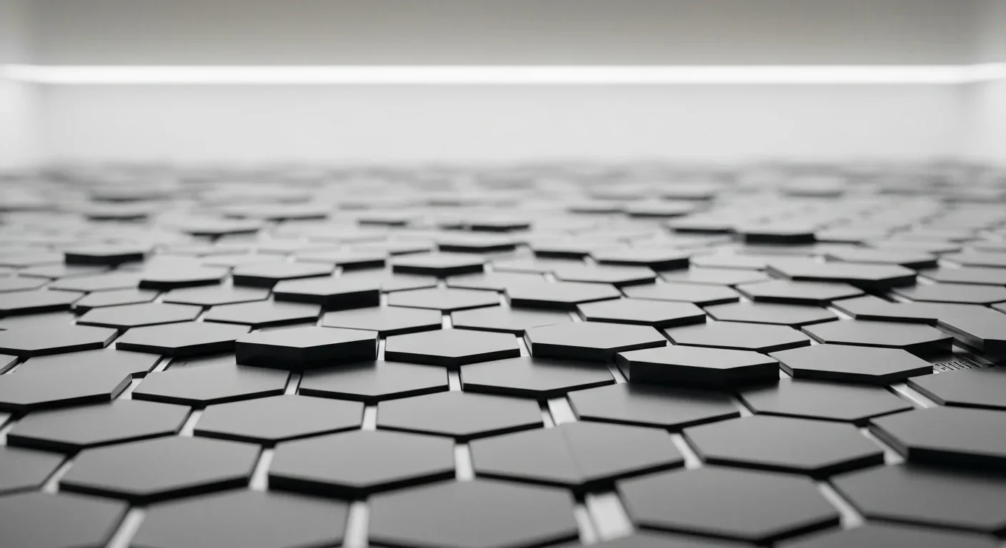
Wafer-on-wafer bonding fuses logic and memory silicon at the atomic level, delivering up to 100x interconnect density over traditional packaging. TSMC, Intel, and Samsung are racing to commercialize the technology as AI chips hit the memory bandwidth wall.

Loading featured articles...