CXL Memory Pooling Ends the Era of Wasted Server RAM

CXL Memory Pooling Ends the Era of Wasted Server RAM
TPM 2.0 Explained: The Security Chip Protecting Your PC

GAA Nanosheet Transistors: Biggest Chip Shift Since 2011
Why Quantum Computers Need 1,000 Qubits for One
TPM 2.0 and Pluton: Hardware Root of Trust Explained
Why Quantum Computing Bet on One Qubit Design
TL;DR: Wafer-on-wafer bonding fuses logic and memory silicon at the atomic level, delivering up to 100x interconnect density over traditional packaging. TSMC, Intel, and Samsung are racing to commercialize the technology as AI chips hit the memory bandwidth wall.

The next technological revolution won't come from shrinking transistors further. It will come from stacking them.
For decades, the semiconductor industry chased a single strategy: make everything smaller. Cram more transistors onto a flat plane of silicon. That strategy has hit a wall, and the consequences touch everything from the AI models running your search queries to the geopolitical standoff over who controls the world's most advanced chips. The answer, increasingly, is to build up instead of out, and a technique called wafer-on-wafer bonding sits at the heart of that vertical revolution.
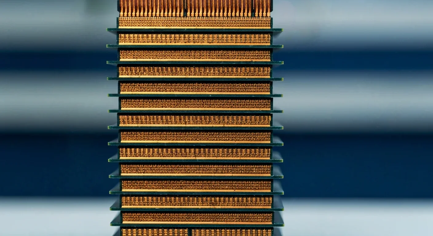
In early 2026, TSMC announced that its SoIC hybrid bonding technology had reached high-volume manufacturing at a 6-micrometer bond pitch. That number might sound abstract, so here's what it means in practice: by eliminating the tiny solder bumps that have connected chips for decades, TSMC unlocked a 100-fold increase in interconnect density compared to conventional microbump packaging. Where traditional approaches pack roughly 600 to 1,000 connections per square millimeter, TSMC's bumpless architecture achieves 25,000 to 50,000 interconnects in the same area.
This isn't incremental improvement. It's a structural shift in how the most powerful processors on Earth are assembled. And it comes at exactly the moment when AI accelerators, high-performance computing systems, and mobile processors are all starving for memory bandwidth they can't get from traditional packaging.
At 6-micrometer pitch, TSMC's bumpless hybrid bonding achieves 25,000 to 50,000 interconnects per square millimeter, compared to just 600 to 1,000 with conventional microbumps. That's up to a 100-fold density increase in the same silicon footprint.
The idea of stacking silicon isn't new. Just as cities grew upward when real estate became too expensive to sprawl outward, chipmakers have been exploring vertical integration since the 1980s. Early approaches were crude: separate packages wired together on a circuit board, burning power to shuttle data across centimeters of copper trace.
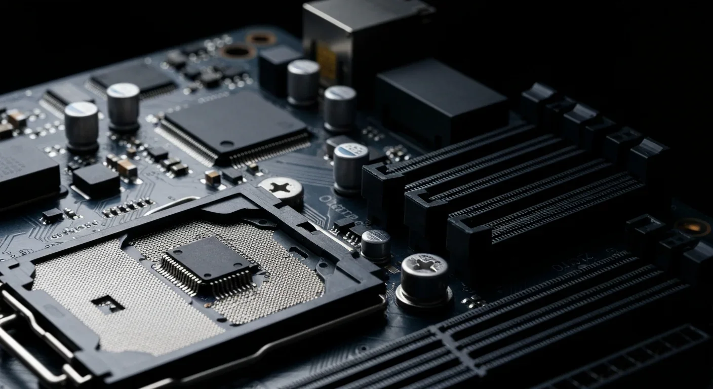
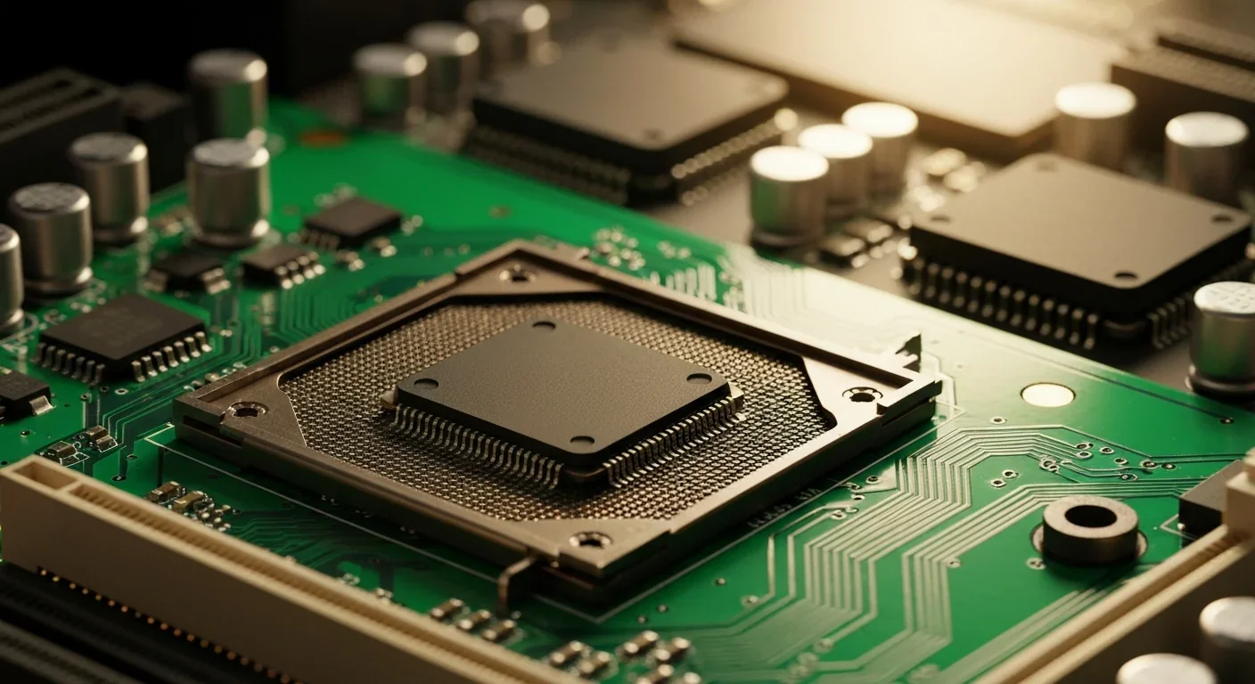
The first real step toward vertical integration came with through-silicon vias, or TSVs, tiny holes drilled through silicon wafers and filled with metal to carry signals vertically. TSVs enabled high bandwidth memory, or HBM, the stacked DRAM technology that powers virtually every major AI accelerator today. NVIDIA's H100 and H200 GPUs, AMD's Instinct MI300 series, and Google's TPUs all rely on HBM stacks connected to logic processors via silicon interposers.
But TSV-based stacking has limits. The vias are relatively large, typically 5 to 10 micrometers in diameter, and they use microbump solder connections that impose a pitch floor around 20 to 50 micrometers. That's not dense enough for what comes next.
The real breakthrough is hybrid bonding, and more specifically, wafer-on-wafer hybrid bonding. Instead of drilling holes and filling them with solder, this approach polishes the copper wiring and oxide insulation layers of two separate wafers to an atomic-level smoothness, less than 0.5 nanometers of roughness. The wafers are pressed together at room temperature, then annealed at around 200 degrees Celsius. The copper atoms in the top and bottom surfaces diffuse and fuse into a single continuous metal path, while the surrounding dielectric material bonds simultaneously. No bumps. No solder. No intermediaries.
The result is interconnect densities 100 to 1,000 times higher than what microbumps can achieve, with power consumption below 0.05 picojoules per bit, roughly 3 to 10 times more efficient than 2.5D alternatives.
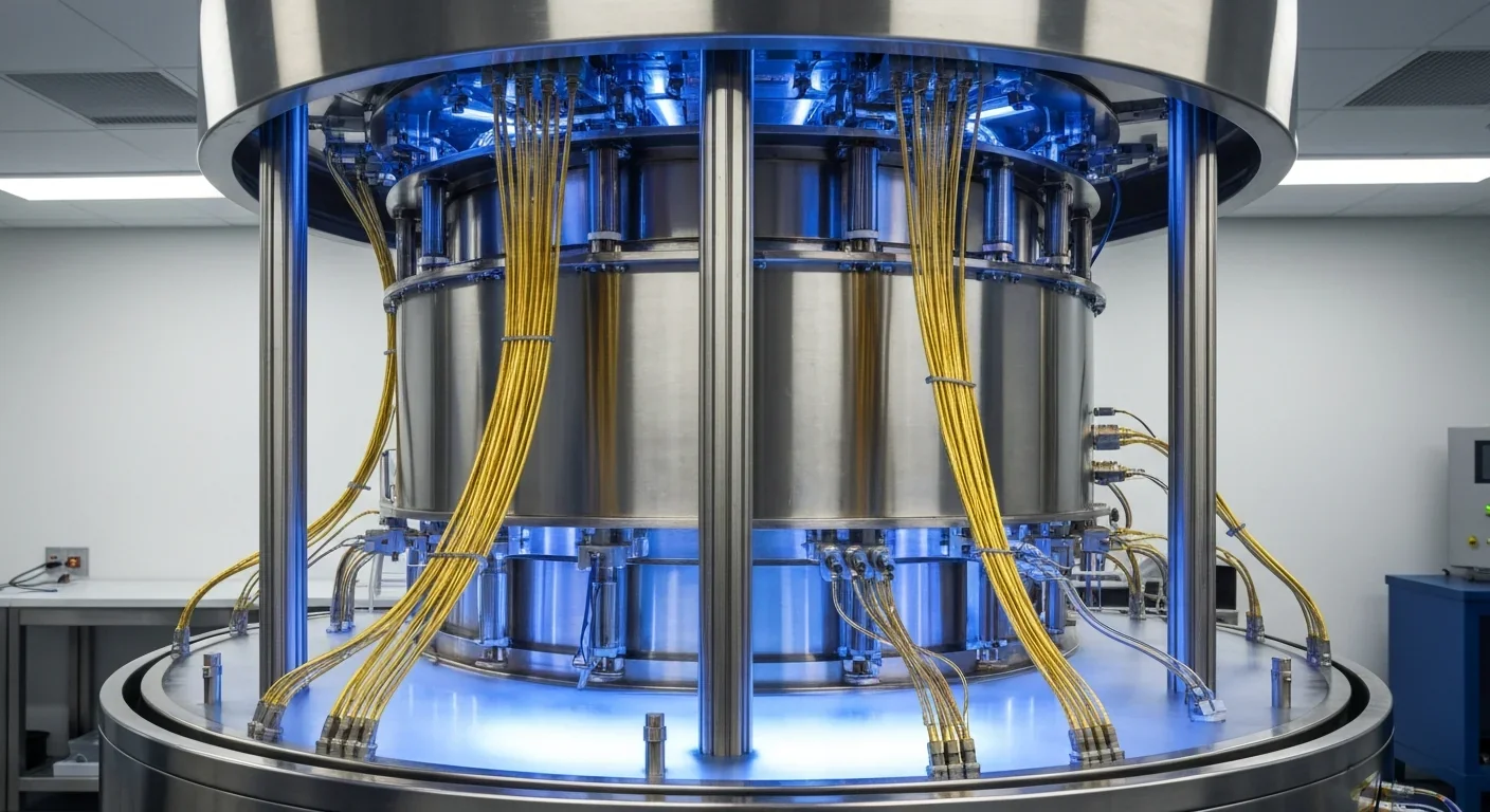
Understanding why this matters requires a brief look at how wafer-on-wafer bonding actually works. The process has three bonding configurations: wafer-to-wafer, die-to-wafer, and die-to-die. Wafer-to-wafer offers the finest achievable pitch because both surfaces can be lithographically aligned with the same equipment used to print the circuits themselves.
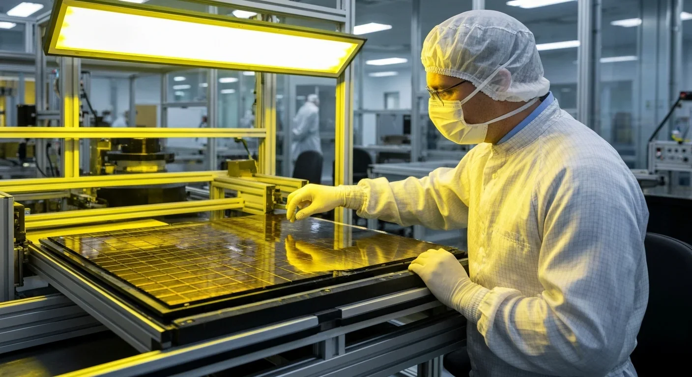
The process starts with chemical-mechanical polishing, or CMP, to achieve mirror-flat surfaces. Cavities are etched into the dielectric, filled with barrier material, seed layers, and copper pads. After plasma activation of the dielectric surface, two 300-millimeter wafers are aligned and pressed together. The initial bond forms at room temperature through van der Waals forces between the activated dielectric surfaces. A subsequent anneal causes the copper pads to expand and form permanent metallic bonds.
The alignment tolerances are extraordinary. At sub-10-micrometer pitches, overlay accuracy must be better than 100 nanometers across a 300-millimeter wafer. IMEC demonstrated reliable 400-nanometer pitch bonding using SiCN dielectric at IEDM 2023 and showed a path to 250-nanometer pitch at VLSI 2025. Commercial production sits at 6 micrometers today; research is already demonstrating pitches 15 times finer.

At 6-micrometer pitch, hybrid bonding achieves roughly 250,000 to 1 million interconnects per square millimeter. Direct copper connections lower both resistance and inductance, enabling memory interfaces capable of multi-terabyte-per-second bandwidth.
"Hybrid bonding is the pinnacle of fine-pitch packaging, minimizing resistance, parasitic capacitance-induced latency, and power consumption while improving thermal performance and bandwidth relative to microbump bonds."
- Jonathan Abdilla, Director of Technology, Besi
Here's where the physics of perfection meets the economics of imperfection. When you bond two complete wafers together before dicing them into individual chips, you multiply their defect rates. If each wafer has a 90% die yield, the bonded pair has roughly an 81% yield before you even account for bonding defects. Stack more layers and the math gets worse: an 8-layer stack with 99% yield per layer drops to 92% overall, and a 12-layer stack falls to 87%.
This is the yield multiplication problem, and it's the single biggest commercial barrier to widespread wafer-on-wafer adoption. A single misaligned bond during annealing can destroy multiple high-value dies. Unlike die-to-wafer bonding, where manufacturers can pre-select known-good dies before bonding, wafer-on-wafer commits every die on both wafers, good and bad alike.
The industry response has been twofold. First, fanatical process control: TSMC's SoIC platform emphasizes meticulous yield management. Second, advanced metrology: EV Group's EVG 40 D2W platform measures 2,800 overlay points across a wafer in four minutes, capturing 100% die positioning data. The tools are improving, but the fundamental math of multiplicative yield loss remains a constraint.
Yield multiplication is wafer-on-wafer bonding's biggest commercial hurdle. Two wafers each yielding 90% produce a bonded pair at just 81%, before any bonding defects are counted. Every additional layer compounds the loss.
The commercial competition in wafer-on-wafer bonding has become a proxy war for semiconductor leadership.
TSMC leads with its SoIC platform, in production since 2022 and achieving 6-micrometer pitch at high volume by early 2026. The latest generation delivers a 1.83-fold increase in bonding density and a 1.96-fold improvement in bandwidth-to-power ratio. NVIDIA's upcoming Rubin platform and AMD's MI400 series are built on this architecture.
Intel is pushing Foveros Direct, targeting a sub-5-micrometer bonding pitch on the 18A-PT process node. Intel's approach combines hybrid bonding with its PowerVia backside power delivery, which reduces IR drop by 122 millivolts and shrinks core area by 22%. Packaging revenue is expected to exceed one billion dollars before wafer manufacturing revenue materializes.
Samsung has demonstrated its X-Cube technology, stacking SRAM on logic dies. But Samsung has not yet reached high-volume production for wafer-on-wafer bonding, leaving it a step behind.
The timing of this technology's maturation isn't accidental. AI workloads are memory-bandwidth-limited.
HBM4, the next generation of high bandwidth memory, doubles the I/O count from 1,024 to 2,048 and can deliver up to 2 terabytes per second of bandwidth per device. A package with eight HBM4 devices offers 512 gigabytes of capacity and more than 16 terabytes per second of aggregate bandwidth, a 2.5-fold increase over HBM3.
But here's the twist: current HBM stacks still use TSV-based microbump connections, not hybrid bonding. The transition to hybrid-bonded HBM is widely expected but hasn't happened in high volume yet. When it does, it will eliminate solder bumps between DRAM layers, allowing for taller stacks, tighter pitches, and bandwidth density that next-generation AI architectures require.
"HBM failures are the number one cause of GPU failures, which happen more frequently than other chips in the data center."
- SemiAnalysis Newsletter
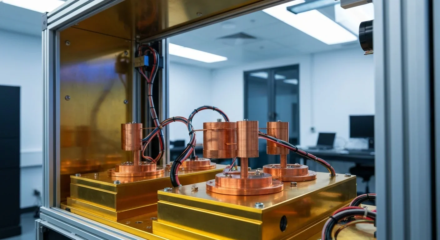
The thermal challenge is real. Stacking high-power logic directly beside memory creates a "heat sandwich." Solutions include microfluidic cooling channels etched into silicon and backside power delivery networks that separate power from signal routing. These technologies are experimental now but will become mandatory.

Advanced packaging has become a strategic frontier in the global semiconductor competition. Export controls on hybrid bonding equipment now extend beyond chip fabrication tools. The CHIPS Act has fueled billions in domestic packaging investments, with Intel positioning itself as the only US-based supplier of both leading-edge process technology and advanced packaging.
Chinese researchers have demonstrated a 3D hybrid-bonded chip stacking 14-nanometer logic on 18-nanometer DRAM, claiming 120 teraflops and 2 teraflops per watt. Whether these claims hold up remains to be seen, but the effort signals that China views 3D integration as a route to competitive AI hardware despite lithography restrictions.
The equipment supply chain is concentrated. Five companies collectively control 60 to 65% of the hybrid bonding equipment market. The global market is expected to grow from $165 million in 2025 to $634 million by 2030, a compound annual growth rate of 21.2%. Access to this equipment is now a matter of national industrial policy.
While IMEC drives fundamental physics forward in Europe, and researchers in Japan and Korea push bonding materials, the commercial battleground remains centered on Taiwan and the United States. The Universal Chiplet Interconnect Express standard promises mix-and-match 3D stacks, but widespread adoption is years away.
Within the next decade, nearly every high-performance processor you interact with will contain vertically stacked silicon bonded at the atomic level. Industry pitches are moving below 10 micrometers today, with roadmaps targeting 3 to 4 micrometers. Research labs have demonstrated sub-500-nanometer bonding. The gap between lab possibilities and fab realities represents both the opportunity and the risk.
The 3D revolution is reshaping the semiconductor value chain, extending from wafer fabrication to back-end assembly and blurring the lines between them. For chipmakers, equipment vendors, and the nations that host them, wafer-on-wafer bonding isn't just a packaging technique. It's the architecture of the AI era, and the race to master it will shape computing for a generation.

Project Orion was a real 1960s program to reach other stars by detonating 800 nuclear bombs behind a spacecraft. The physics worked and the engineering was feasible, but the 1963 nuclear test ban treaty killed it. It remains the most credible interstellar spacecraft ever designed.

The locus coeruleus, a tiny brainstem structure, degenerates decades before Alzheimer's symptoms appear. Its loss cripples the brain's inflammation control, waste clearance, and sleep regulation. New imaging tools and noradrenergic therapies offer hope for early detection and prevention.

Research shows the sharing economy often increases total resource consumption through the Jevons paradox and rebound effects. Ride-sharing adds billions of vehicle miles, co-working spaces use more energy per worker, and diffused responsibility erodes conservation behavior. Breaking the paradox requires congestion pricing, accountability design, and matching sharing models to appropriate resource types.

Psychological reactance theory explains why banning or restricting things makes people want them more. From Prohibition to the Streisand effect to scarcity marketing, research shows that threatening people's freedom reliably backfires, and autonomy-supportive communication is far more effective.

A carnivorous pitcher plant in Borneo evolved to house bats instead of trapping insects, gaining up to 95% of its nitrogen from bat guano. The plant even built an ultrasonic reflector to help bats find it, revealing that carnivory in plants is a flexible spectrum.
The quantified self movement began as a hacker-ethos pursuit of personal insight, but corporate wearables now funnel biometric data to employers, insurers, and data brokers. With 81% of Americans wrongly believing health apps are HIPAA-protected, a regulatory void enables health data to be sold for pennies while generating anxiety instead of empowerment.
CXL memory pooling lets servers dynamically share DRAM over a cache-coherent interconnect, eliminating the 40% stranded memory waste in data centers. With commercial hardware now shipping and Azure deploying CXL cloud instances, this technology promises to cut memory costs by 50% while enabling composable infrastructure.

Loading featured articles...