CXL Memory Pooling Ends the Era of Wasted Server RAM

CXL Memory Pooling Ends the Era of Wasted Server RAM
TPM 2.0 Explained: The Security Chip Protecting Your PC

Wafer-on-Wafer Bonding Breaks AI's Bandwidth Wall
Why Quantum Computers Need 1,000 Qubits for One
TPM 2.0 and Pluton: Hardware Root of Trust Explained
Why Quantum Computing Bet on One Qubit Design
TL;DR: Gate-all-around nanosheet transistors are replacing FinFETs as the dominant chip architecture, wrapping the gate around the entire channel for dramatically better power efficiency and performance. Samsung shipped first in 2022, TSMC followed at 2nm in 2025, and Intel pairs its RibbonFET with backside power delivery.

The next technological revolution won't arrive as a flashy gadget or a viral app. It's happening right now, inside factories where silicon wafers spin under ultraviolet light, and the stakes couldn't be higher. The transistor, that invisible switch powering every smartphone, data center, and AI model you've ever used, is getting its most radical redesign in over a decade. Gate-all-around nanosheet transistors are replacing the FinFET architecture that has dominated advanced chip manufacturing since Intel's 22nm Ivy Bridge processors hit the market in 2012. And the implications ripple far beyond the semiconductor cleanroom.
To understand why this matters, you need to know what FinFETs actually solved. Before 2011, transistors were flat. The gate sat on top of a planar channel, controlling current flow from above. As these planar transistors shrank below 30nm, the gate lost its grip on the channel. Electrons leaked through like water through a cracked dam, wasting power and generating heat.
Intel's solution was elegant. The FinFET raised the channel into a thin vertical fin, allowing the gate to wrap around it on three sides. This tri-gate design dramatically improved electrostatic control, reduced leakage, and enabled faster switching. It was a breakthrough that powered the entire smartphone era, from the iPhone 5 through today's AI accelerators.
Every major chipmaker followed Intel's lead. Samsung, TSMC, and GlobalFoundries all adopted FinFET variants. For over a decade, the architecture scaled beautifully from 22nm down through 7nm and even 5nm nodes. But physics doesn't negotiate.
Below 5nm, the FinFET's three-sided gate coverage isn't enough. The bottom of the fin, where it connects to the substrate, becomes an uncontrolled leakage path. Short-channel effects come roaring back. Drain-induced barrier lowering increases. The sub-threshold swing degrades. Quantum tunneling from source to drain becomes significant. In practical terms, chips leak too much power, run too hot, and can't deliver the performance gains that each new node is supposed to bring.
The industry needed something fundamentally different. Not a tweak to FinFET, but a new geometry entirely.
Below 5nm, the FinFET's three-sided gate can't control the bottom of the fin. That uncontrolled region becomes a leakage path so severe that it erases the power and performance gains each new node is supposed to deliver.
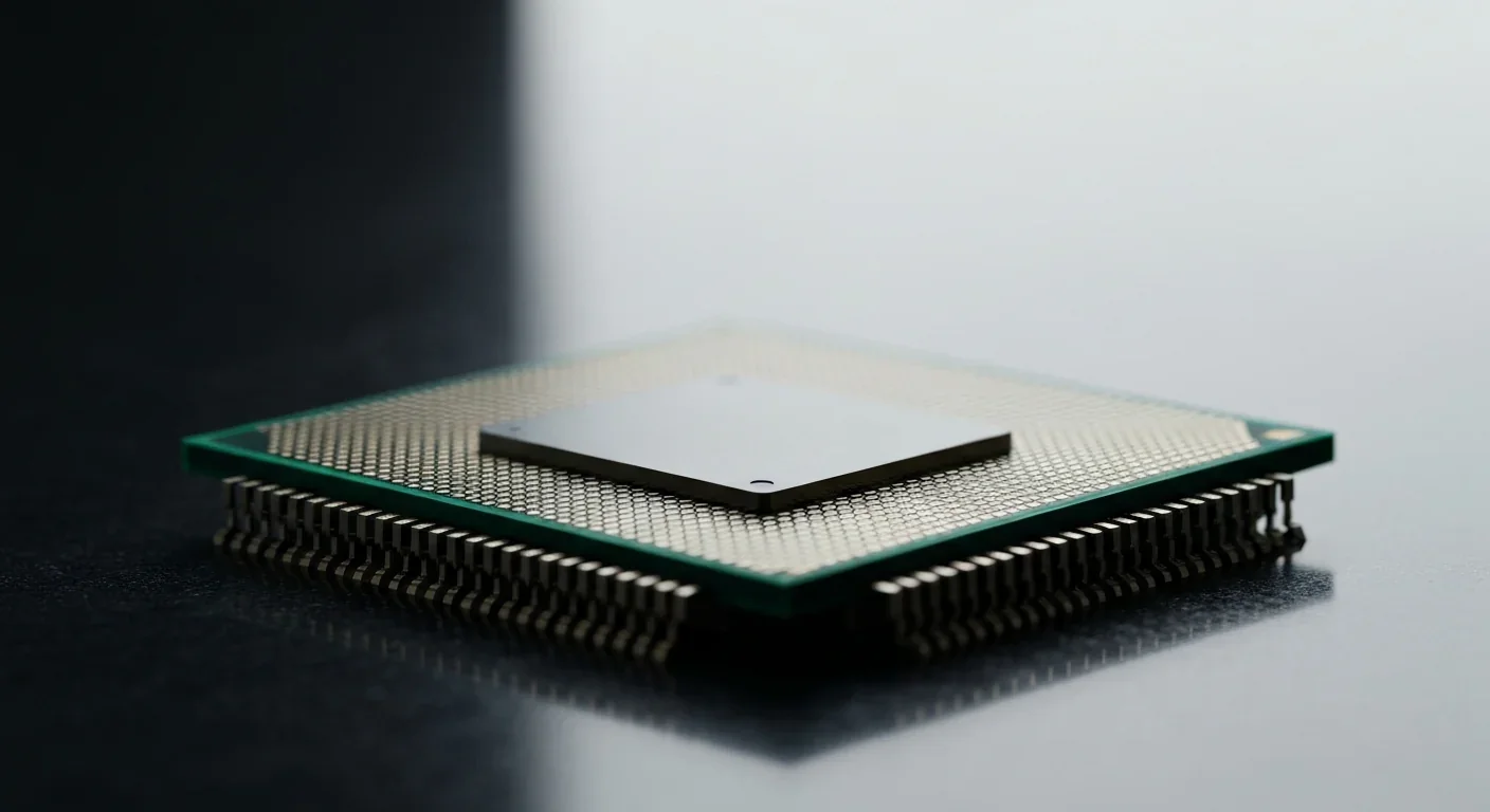
Gate-all-around nanosheet transistors solve the FinFET's core weakness with a conceptually simple idea: instead of wrapping the gate around three sides of a fin, wrap it around the entire channel. Picture stacking several thin, flat silicon ribbons horizontally, then surrounding each one completely with gate material. That's a GAA nanosheet transistor.
The electrostatic advantages are significant. Where FinFETs achieve DIBL values of roughly 60 to 80 millivolts per volt, GAA nanosheets bring that down to 30 to 45 millivolts per volt. Sub-threshold swing improves from 75-85 millivolts per decade to 65-70 millivolts per decade. Leakage current drops by 3.7 to 4 times. These aren't incremental improvements. They represent a step-function change in how effectively the transistor switches between on and off states.
There's another benefit that chip designers particularly love. FinFETs come in fixed heights, so you adjust drive current by adding or removing entire fins, a quantized, coarse adjustment. GAA nanosheets let you vary the width of each sheet continuously, giving designers fine-grained control over drive current and leakage. It's like going from a dimmer switch with three settings to one with infinite resolution.
Researchers have demonstrated GAAFETs with up to seven stacked nanosheets, though current production designs typically use three to four sheets. More sheets mean more drive current, but also more manufacturing complexity, a tradeoff the industry is still optimizing.
Samsung made history in June 2022 when it began risk production of 3nm GAA chips using its Multi-Bridge Channel FET (MBCFET) architecture. It was the first foundry in the world to ship GAA transistors at commercial scale, and the performance numbers were promising: up to 45% power reduction, 23% performance improvement, and 16% area reduction compared to its 5nm FinFET.
But being first came with costs. Samsung's initial 3GAE yields were significantly lower than its mature 5nm FinFET line. Even by 2025, reports from South Korean media indicated yields stuck around 50%, while TSMC's 3nm FinFET process achieved over 90%. That gap pushed major customers like Google, Qualcomm, and AMD toward TSMC, while Samsung's early 3nm GAA production remained largely limited to internal projects and cryptocurrency ASICs.
"N2 is well on track for volume production later this quarter, with good yield. We expect a faster ramp-up in 2026, fueled by both smartphone and HPC AI applications."
- C.C. Wei, Chief Executive Officer, TSMC
Intel took a different path. Rather than rushing GAA to market, the company chose to extract maximum performance from its remaining FinFET nodes before introducing its GAA implementation, called RibbonFET. Intel's design uses four stacked nanosheets per transistor and pairs the architecture with PowerVia, a backside power delivery network that routes power through the back of the wafer instead of competing for space with signal wires on the front. This combination, planned for the Intel 18A node, represents a dual innovation that could significantly improve both transistor density and power efficiency.
TSMC, the world's largest contract chipmaker, was the most conservative. It kept FinFET technology for its entire 3nm family of nodes, including N3, N3E, and N3P, before making the GAA leap at 2nm. TSMC's N2 node entered volume production in late 2025, offering a 10-15% speed improvement and 25-30% power reduction over N3E. TSMC plans to ramp to 40,000 wafers per month in 2025, scaling to 200,000 by 2027.
For Apple, AMD, and Nvidia, all major TSMC customers, this transition means their next generation of processors and GPUs will be built on GAA technology.

Building GAA nanosheets is dramatically harder than building FinFETs. The process introduces entirely new fabrication steps that have no equivalent in traditional FinFET manufacturing.
It starts with growing alternating layers of silicon and silicon-germanium in a precise superlattice structure. Each layer must be uniform in thickness across the entire wafer, a tolerance measured in individual atomic layers. Then comes the channel release etch, the most critical and unique step. You need to selectively dissolve the silicon-germanium sacrificial layers while leaving the silicon nanosheets perfectly intact and suspended. Any over-etching damages the channel. Any under-etching leaves residue that degrades performance.
Inner spacer formation follows, isolating the gate from the source and drain regions. These spacers must be precise enough to suppress parasitic capacitance and leakage without increasing the gate pitch. Finally, the gate stack itself must be deposited uniformly around each suspended nanosheet using atomic layer deposition, all under tight thermal budgets that won't damage previously formed structures.
Manufacturing GAA nanosheets requires process steps with no equivalent in FinFET fabrication: superlattice growth, selective channel release etching, inner spacer formation, and conformal gate deposition around suspended structures only a few atoms thick.
And underneath all of this sits extreme ultraviolet lithography. EUV, produced exclusively by the Dutch firm ASML, uses 13.5nm wavelength light to pattern features that conventional optical lithography simply cannot resolve. Current EUV tools operate at 0.33 numerical aperture, but the next generation of high-NA EUV at 0.55 NA is expected to simplify patterning for GAA structures at 2nm and below. Intel has already partnered with ASML to deploy high-NA EUV for its future nodes.
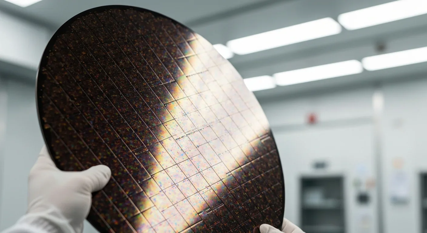
The fact that only three companies in the world, TSMC, Samsung, and Intel, can manufacture chips below 7nm tells you something about the barriers to entry in advanced semiconductors. The GAA transition raises those barriers even higher.
ASML's monopoly on EUV lithography has become a major geopolitical concern. Each EUV machine costs roughly $180 million, and only about 2% of the source light actually reaches the wafer. High-NA EUV tools are even more expensive. Governments from Washington to Beijing to Brussels understand that controlling access to these machines means controlling who can build cutting-edge chips.
The GAA transistor market itself is projected to grow from roughly $600 million in 2024 to over $2 billion by 2034, with Asia Pacific holding about 60% of the market. But the real economic impact is measured in the trillions of dollars of products those chips enable, from AI training clusters to autonomous vehicles to next-generation smartphones.
"EUV lithography machines are famously made by just a single firm, ASML in the Netherlands, and determining who has access to the machines has become a major geopolitical concern."
- Brian Potter, Construction Physics
While Silicon Valley and Seoul race to perfect nanosheet manufacturing, researchers in Tokyo and across Europe are exploring the complementary FET (CFET) architecture that could follow GAA. CFETs stack an NMOS transistor directly on top of a PMOS transistor, potentially doubling density again. Combined with 2D materials like molybdenum disulfide for ultra-thin channels, the roadmap beyond initial GAA nodes is already taking shape.
Within the next two to three years, the phone in your pocket, the laptop on your desk, and the cloud servers processing your data will all run on GAA transistors. The performance and power improvements translate directly into longer battery life, faster processing, and AI capabilities that today's hardware can't support.
But the shift also concentrates even more technological power in fewer hands. The cost of building a leading-edge fab has crossed $20 billion. The expertise required to manufacture nanosheet transistors represents decades of accumulated knowledge that can't be replicated quickly. And the supply chain dependencies, from ASML's lithography tools to specialty chemical suppliers, create fragilities that pandemics and geopolitical tensions have already exposed.
The GAA transition isn't just a technical milestone. It's a civilizational one, a reminder that the most consequential technologies are often the ones you never see. Somewhere right now, in a cleanroom in Taiwan, a nanosheet just a few atoms thick is being carved from silicon, wrapped in metal, and wired into a circuit that will help shape the future. The biggest change in transistor design since 2011 is here. And it's only the beginning.
Project Orion was a real 1960s program to reach other stars by detonating 800 nuclear bombs behind a spacecraft. The physics worked and the engineering was feasible, but the 1963 nuclear test ban treaty killed it. It remains the most credible interstellar spacecraft ever designed.

The locus coeruleus, a tiny brainstem structure, degenerates decades before Alzheimer's symptoms appear. Its loss cripples the brain's inflammation control, waste clearance, and sleep regulation. New imaging tools and noradrenergic therapies offer hope for early detection and prevention.

Research shows the sharing economy often increases total resource consumption through the Jevons paradox and rebound effects. Ride-sharing adds billions of vehicle miles, co-working spaces use more energy per worker, and diffused responsibility erodes conservation behavior. Breaking the paradox requires congestion pricing, accountability design, and matching sharing models to appropriate resource types.

Psychological reactance theory explains why banning or restricting things makes people want them more. From Prohibition to the Streisand effect to scarcity marketing, research shows that threatening people's freedom reliably backfires, and autonomy-supportive communication is far more effective.

A carnivorous pitcher plant in Borneo evolved to house bats instead of trapping insects, gaining up to 95% of its nitrogen from bat guano. The plant even built an ultrasonic reflector to help bats find it, revealing that carnivory in plants is a flexible spectrum.

The quantified self movement began as a hacker-ethos pursuit of personal insight, but corporate wearables now funnel biometric data to employers, insurers, and data brokers. With 81% of Americans wrongly believing health apps are HIPAA-protected, a regulatory void enables health data to be sold for pennies while generating anxiety instead of empowerment.
CXL memory pooling lets servers dynamically share DRAM over a cache-coherent interconnect, eliminating the 40% stranded memory waste in data centers. With commercial hardware now shipping and Azure deploying CXL cloud instances, this technology promises to cut memory costs by 50% while enabling composable infrastructure.

Loading featured articles...