Wafer-on-Wafer Bonding Breaks AI's Bandwidth Wall
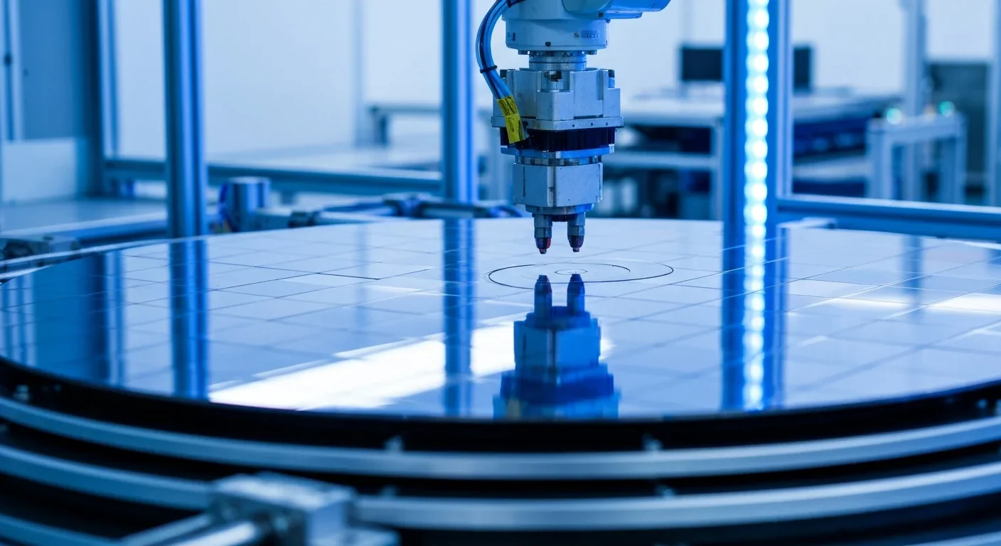
Wafer-on-Wafer Bonding Breaks AI's Bandwidth Wall
Why Quantum Computers Need 1,000 Qubits for One
TPM 2.0 and Pluton: Hardware Root of Trust Explained
Why Quantum Computing Bet on One Qubit Design

P4 Programmable Switches Rewriting Networks at Tbps
Intel TSX Failed. Can ARM Fix Transactional Memory?
TL;DR: MRAM has finally crossed from laboratory curiosity to commercial reality, with Samsung, TSMC, and GlobalFoundries shipping embedded MRAM in automotive, IoT, and edge AI products. The market could reach $58 billion by 2035 as MRAM replaces embedded Flash in microcontrollers.

The next technological revolution in computing won't come from faster processors or bigger hard drives. It will come from memory that never forgets, boots instantly, and barely sips power. After nearly four decades of laboratory tinkering, magnetoresistive random access memory, or MRAM, is finally shipping in real products, powering everything from autonomous vehicles to satellites. And the implications reach far beyond silicon.
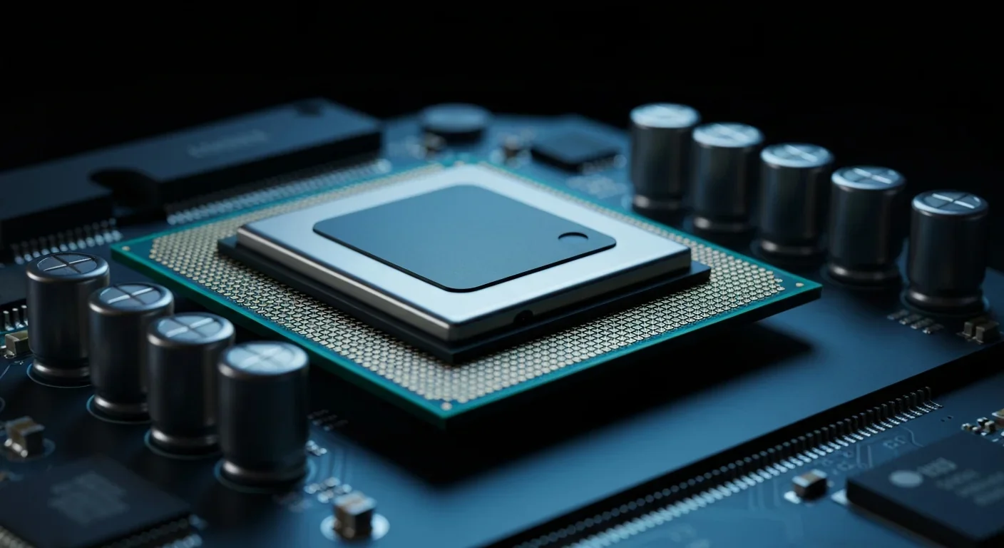
To understand why MRAM matters, you need to understand a tiny sandwich. A magnetic tunnel junction, or MTJ, consists of two ferromagnetic layers separated by an ultra-thin magnesium oxide barrier roughly one nanometer thick. Electrons tunnel through this barrier, and the electrical resistance changes dramatically depending on whether the magnetic layers point in the same direction or opposite ones. This phenomenon, called tunnel magnetoresistance, is what makes reading data from an MRAM cell possible.
The breakthrough moment came in 2004, when researchers Shinji Yuasa and Stuart Parkin independently demonstrated that crystalline MgO barriers could achieve tunnel magnetoresistance ratios exceeding 200% at room temperature. By 2008, CoFeB/MgO/CoFeB junctions had pushed that figure past 604% at room temperature. This wasn't incremental improvement. Earlier amorphous aluminum oxide barriers had maxed out around 70%. The jump to MgO was like going from a walkie-talkie to a smartphone, a completely different order of capability enabled by a quantum mechanical trick called symmetry filtering, where the crystalline structure of MgO selectively allows only certain electron states to pass through.
But high TMR ratios were only half the puzzle. Writing data reliably required its own revolution. Enter spin-transfer torque, a method where a spin-polarized electric current directly flips the magnetic state of the storage layer without needing external magnetic fields. STT-MRAM, as it became known, slashed write energy, improved scalability, and opened the door to embedding MRAM directly inside processor chips.
The history of MRAM reads like a patience test for the semiconductor industry. The concept dates back to the 1980s, when researchers first realized that magnetoresistance could encode digital information. Motorola built early prototypes in the late 1990s. But for years, MRAM occupied that awkward middle ground, too expensive for mass production, too promising to abandon.
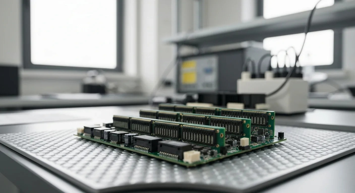
The real inflection point was commercial. In 2006, Everspin Technologies, spun off from Freescale Semiconductor, became the first company to ship standalone MRAM products. Their early toggle-MRAM devices proved the technology could survive outside a research lab. Then in 2012, Everspin released a 64 Mb DDR3 STT-MRAM module, the first commercially available product using the newer spin-transfer torque approach.
Samsung followed in 2019, shipping embedded STT-MRAM in production using a 28nm process. That was a signal the rest of the industry couldn't ignore. When the world's largest memory manufacturer commits to volume production, it changes the calculus for everyone.
Today, the foundry ecosystem has organized around MRAM. TSMC offers embedded MRAM at its 22nm ultra-low-power process node. GlobalFoundries provides eMRAM on its 22FDX platform targeting IoT and automotive markets. Samsung has pushed even further, demonstrating 128 Mb embedded MRAM at 8nm with sub-ppm failure rates and stable operation from -40 to 150 degrees Celsius.
Just as the printing press didn't just copy manuscripts but fundamentally reorganized how knowledge spread, MRAM isn't just replacing existing memory. It's enabling entirely new computing architectures that weren't possible before.
The memory landscape has long been defined by painful trade-offs. SRAM is fast but expensive and power-hungry. DRAM is dense but volatile, requiring constant refresh cycles that consume up to 99% more power than necessary. NOR Flash retains data without power but wears out after roughly 100,000 write cycles and operates at glacial speeds compared to SRAM.
MRAM breaks these trade-offs in ways that matter. Read access times fall in the 2 to 10 nanosecond range, approaching SRAM performance. IBM has demonstrated devices hitting 2 nanosecond access times. Write endurance exceeds 10^12 cycles, meaning you could write to an MRAM cell once per second for 30,000 years before it wore out. And because MRAM stores data magnetically, it never requires refresh and retains information with the power turned off.
There's a concept that engineers call the "pentalemma," five competing demands that every memory technology must balance: retention, speed, endurance, read disturbance, and process integration. No technology wins on every dimension. But MRAM comes closer than anything else to being a universal memory, one that combines the speed of SRAM, the density approaching DRAM, and the persistence of Flash.
Against other emerging technologies, MRAM also holds advantages. ReRAM, or resistive RAM, offers good density but struggles with endurance variability. Phase-change memory, or PCM, has found a niche in CXL memory expanders for data centers but requires high write temperatures. The combined market for MRAM, PCM, and ReRAM is projected to exceed $36 billion by 2030, but MRAM is capturing the lion's share of design wins in safety-critical applications.
Perhaps the most commercially significant development is what's happening inside microcontrollers. For decades, embedded NOR Flash has been the default non-volatile memory in MCUs. But there's a problem: scaling embedded Flash below 28nm requires additional costly mask layers, adding 15 to 20% to manufacturing costs. Below that node, the physics simply stop cooperating.
This is where embedded MRAM steps in. Because MRAM can be integrated into standard CMOS manufacturing at 65nm, 40nm, 28nm, and now 22nm nodes, it avoids the scaling wall that Flash has hit. The advantages go beyond cost. Embedded MRAM offers higher endurance, faster writes, no erase cycles needed, byte addressability, lower leakage, and lower manufacturing costs compared to Flash.
"Embedded MRAM satisfies ISO 26262 functional-safety needs, offers instant-on behavior, and delivers unlimited write endurance."
- NXP Semiconductors
Renesas has made this concrete with its RA8 series MCUs, which integrate 1 MB of high-speed MRAM alongside 2 MB of SRAM on a 22nm process. These chips target industrial automation, automotive systems, and IoT edge devices. NXP Semiconductors and TSMC have announced development of 16nm FinFET embedded MRAM for automotive applications, pushing the technology toward even more advanced nodes.
MRAM's toughness makes it uniquely suited for environments where other memories fail. The technology retains data for more than 10 years at temperatures up to 150 degrees Celsius, meeting the stringent qualification requirements of the automotive industry. It can resist high ionizing radiation and withstand physical shock, making it ideal for aerospace and military applications.
At the 2025 MRAM Global Innovation Forum, Allen Wang from TSMC presented work showing that N16 MRAM meets Autograde-1 quality standards with a cumulative failure rate below 1 part per million, surpassing other non-volatile memories in manufacturing yield and speed. GlobalFoundries demonstrated a 4 MB automotive MRAM block on 22nm FDSOI with robust performance across wide voltage and temperature ranges.
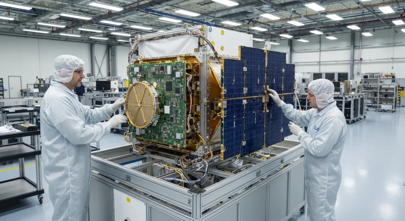
Avalanche Technology has developed radiation-hardened MRAM products designed for harsh environments, while Teledyne e2V provides MRAM for defense avionics operating across military temperature ranges. MRAM is gradually increasing its presence in aviation, providing higher-density non-volatile memory for aircraft black boxes.
For autonomous vehicles, the appeal is especially clear. Software-defined vehicles need memory that boots instantly for safety-critical functions, handles extreme temperature swings under the hood, and endures billions of write cycles from continuously updating sensor data. MRAM checks every box.
While Silicon Valley and its East Asian partners have dominated MRAM development, the competitive landscape is shifting. In a major development, Shanghai Siproin Microelectronics began shipping China's first STT-MRAM chips, manufactured on SMIC's 40nm process. This suggests that Chinese foundries have mastered the manufacturing processes behind STT-MRAM.
Siproin's progress fits into a broader Chinese memory push, joining CXMT's DRAM and YMTC's 3D NAND to form an increasingly complete domestic memory ecosystem. The timing is significant: U.S. export controls are accelerating China's drive for semiconductor independence, and MRAM represents a technology where catching up is feasible because the manufacturing nodes involved are well within Chinese foundry capabilities.
The MRAM competitive landscape is fracturing into three tiers: established leaders like Samsung, TSMC, and GlobalFoundries pushing advanced nodes; Everspin as the standalone specialist; and emerging Chinese competitors building domestic supply chains on mature processes.
In Europe, French startup Antaios secured $11 million in funding to develop spin-orbit torque MRAM, a next-generation variant that promises even faster switching. Researchers in Japan, where much of the foundational TMR physics was discovered, continue pushing boundaries. At IEEE's International Electron Devices Meeting, TSMC and Taiwan's ITRI demonstrated a novel circular-shaped SOT-MRAM device with built-in magnetic anisotropy.
For all its promise, MRAM still faces real hurdles. Density remains the biggest gap. While Everspin ships 1 Gb standalone STT-MRAM, that's tiny compared to the multi-gigabyte DRAM chips and terabyte-scale Flash storage common today. MRAM won't replace your laptop's main memory or your phone's storage anytime soon.
Cost per bit remains higher than both DRAM and Flash, though the gap narrows in embedded applications where Flash scaling costs are rising rapidly. Write energy at advanced nodes presents an ongoing challenge. NIST researchers have found that many experimental devices do not necessarily switch reliably at the levels required by the microelectronics industry, highlighting the need for tighter process control in commercial fabs.
The industry describes these interconnected challenges as the MRAM "pentalemma," balancing retention, speed, endurance, read disturbance, and manufacturing integration simultaneously. Improve one parameter and you often degrade another. Defect engineering, particularly controlling boron diffusion and oxygen vacancies in MgO barriers, remains critical for maintaining consistent performance as device dimensions shrink.

The financial projections tell a story of explosive growth. The global MRAM market was valued at approximately $3.1 billion in 2025 and is projected to reach $58.1 billion by 2035, growing at a compound annual rate of 32.8%. Other estimates are more conservative, with Verified Market Research projecting $6.7 billion by 2030 at a 13.4% CAGR. The variance reflects genuine uncertainty about adoption speed, but the direction is unanimous.
This growth sits within a broader semiconductor memory market expanding from $103 billion to $134 billion by 2030, driven by AI, 5G, and cloud infrastructure. MRAM's share is still small, but its growth rate dwarfs the overall market. The next-generation non-volatile memory market, which includes MRAM, ReRAM, and PCM, is predicted to reach $38.6 billion by 2035.
"MRAM stands out because it delivers SRAM-like performance while being non-volatile, with end-use retention exceeding a decade."
- Dr. Jin-Woo Kim, VP Business Development, Everspin Technologies
Investment activity confirms the momentum. NXP committed $17.5 million to Israeli SOT-MRAM startup RAAAM. Samsung's acquisition of Grandis back in 2011 now looks prescient, having given them early access to the STT-MRAM IP that underpins their current production lines.
Within the next decade, you'll likely interact with MRAM without knowing it. Your car's safety systems will boot instantly because they don't need to load data from Flash. Your IoT sensors will run for years on a single battery because their memory never needs refresh. Edge AI devices will process data locally with instant-on, non-volatile architectures that reduce boot times and accelerate inference.
The bigger shift is architectural. MRAM fits into emerging heterogeneous memory hierarchies where different memory types serve different roles. Rather than a single universal memory, future systems will use SRAM for the fastest cache, MRAM for persistent cache and embedded storage, DRAM for bulk working memory, and Flash or PCM for cold storage. MRAM's unique position as a persistent cache that eliminates refresh cycles simplifies memory controller design and opens pathways for computing-in-memory paradigms.
The convergence of MRAM with computing-in-memory architectures suggests something more fundamental: a shift toward non-volatile computing where the boundary between storage and processing blurs entirely. Imagine devices that never truly turn off, that pick up exactly where they left off with zero latency, that process data right where it's stored.
MRAM spent 40 years as the technology that was always five years away. That era is over. The chips are shipping, the foundries are committed, and the applications are multiplying. The magnetic memory revolution didn't arrive with a bang. It arrived with a spin-polarized current through a one-nanometer tunnel barrier, and it's about to change how every electronic device on the planet remembers.

Saturn's moon Titan may harbour liquid water beneath its frozen crust, kept from freezing by ammonia acting as a natural antifreeze. New Cassini data suggests the interior could be slush with warm water pockets rather than a global ocean, and NASA's Dragonfly mission launching in 2028 aims to investigate whether this exotic environment could support life.

The cerebellum, long dismissed as merely a motor coordinator, forms dense circuits with the prefrontal cortex that shape cognition and emotion. Disruption of these pathways is now linked to schizophrenia, autism, and ADHD, opening new frontiers in diagnosis and non-invasive brain stimulation therapies.

Research shows the sharing economy often increases total resource consumption through the Jevons paradox and rebound effects. Ride-sharing adds billions of vehicle miles, co-working spaces use more energy per worker, and diffused responsibility erodes conservation behavior. Breaking the paradox requires congestion pricing, accountability design, and matching sharing models to appropriate resource types.

Illusory superiority causes most people to rate themselves above average in driving, intelligence, and ethics. This bias is rooted in metacognitive blind spots, shaped by culture, and carries real costs in healthcare, finance, and leadership. Structured feedback and institutional safeguards can help, but require ongoing effort.

Eastern skunk cabbage generates its own body heat through the alternative oxidase pathway, maintaining temperatures up to 35°C above freezing air and melting surrounding snow. This thermogenic ability, shared by roughly 90 plant species worldwide, reveals a level of metabolic sophistication that challenges assumptions about plant passivity.

America has 28 vacant homes for every homeless person, yet homelessness hit record highs in 2024. Speculative investment, geographic mismatches, and political barriers explain the paradox, while Finland and Vienna show that Housing First and social housing models can work when the political will exists.
Wafer-on-wafer bonding fuses logic and memory silicon at the atomic level, delivering up to 100x interconnect density over traditional packaging. TSMC, Intel, and Samsung are racing to commercialize the technology as AI chips hit the memory bandwidth wall.

Loading featured articles...