Wafer-on-Wafer Bonding Breaks AI's Bandwidth Wall
Wafer-on-Wafer Bonding Breaks AI's Bandwidth Wall
Why Quantum Computers Need 1,000 Qubits for One
TPM 2.0 and Pluton: Hardware Root of Trust Explained
Why Quantum Computing Bet on One Qubit Design
P4 Programmable Switches Rewriting Networks at Tbps
Intel TSX Failed. Can ARM Fix Transactional Memory?
TL;DR: Google's TPU pods connect up to 9,216 custom AI chips using optical circuit switches and 3D torus topology, delivering 42 exaflops while consuming 60-65% less energy than GPU alternatives. This infrastructure powers Gemini and other frontier models.
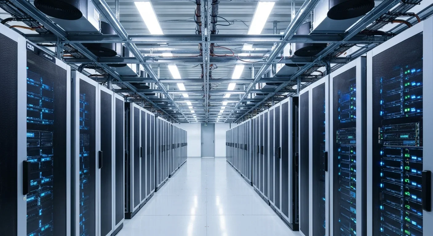
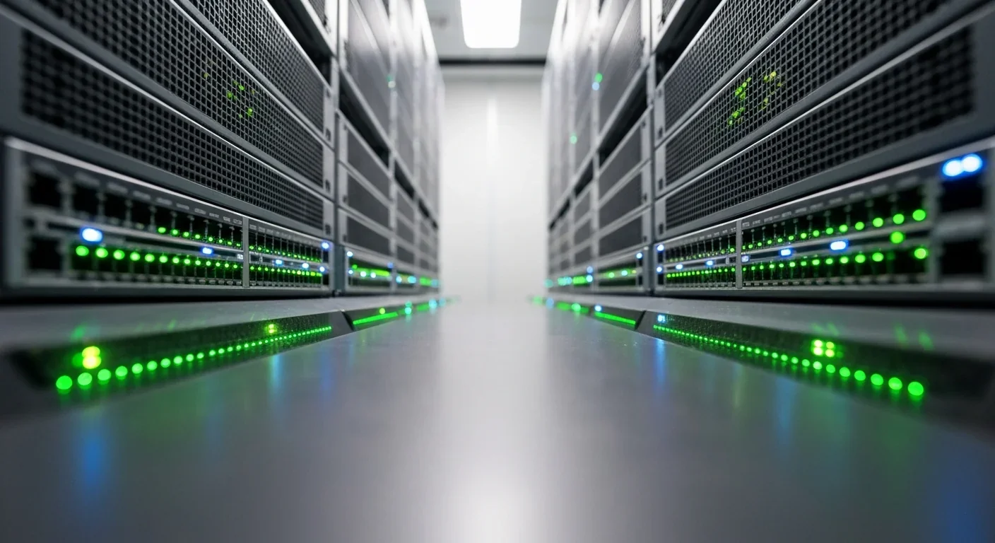
The infrastructure powering today's most advanced AI models isn't some abstract cloud concept. It's thousands of custom silicon chips arranged in a massive three-dimensional mesh, communicating through optical circuit switches at speeds that make traditional networking look glacial. When Google trained Gemini, when it processed billions of images, when it made AlphaGo defeat the world Go champion, the computational heavy lifting happened inside these TPU pods - purpose-built supercomputers that represent a fundamentally different approach to scaling AI hardware.
This isn't just another data center story. Google's Tensor Processing Unit (TPU) pods challenge the prevailing wisdom that Nvidia GPUs are the only game in town for AI infrastructure. While the industry obsesses over GPU shortages and expensive clusters, Google has quietly built what may be the most efficient AI training infrastructure on Earth, and it's changing the economics of how we think about machine learning at scale.
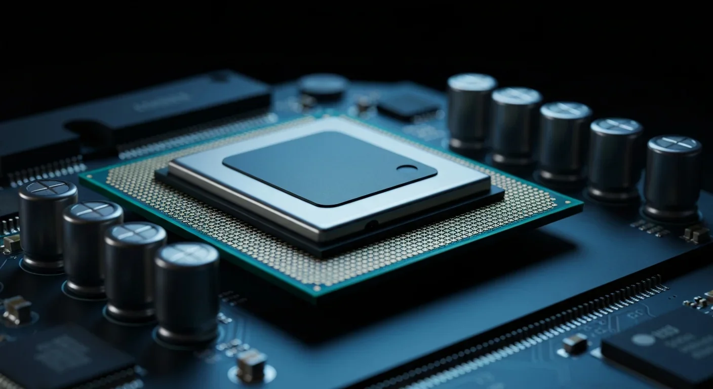
Google didn't set out to build supercomputers. The first TPU, launched in 2015, was designed to solve a specific problem: running inference for Google's neural networks more efficiently than GPUs. The chip was built around a systolic array architecture - a grid of arithmetic units that processes matrix operations by passing data through neighboring units, rather than constantly writing to and reading from memory.
That first generation was inference-only and could handle 92 teraFLOPS of computation. But Google quickly realized that training models, not just running them, was becoming the real bottleneck. TPU v2, released in 2017, added training capabilities and something more ambitious: the ability to link chips together into pods. Those early pods contained 256 chips arranged in modules, delivering 11.5 petaFLOPS of performance - roughly equivalent to a small supercomputer.
With each generation, Google pushed the pod boundaries further. TPU v3 scaled to 2,048 chips using a 3D torus network topology. TPU v4 reached 4,096 chips per pod, a milestone that represented more than just incremental improvement - it required rethinking how thousands of processors coordinate during training.
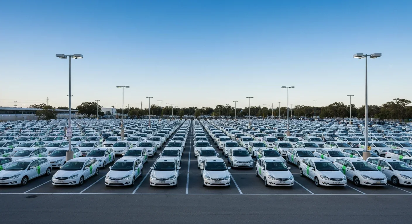
The latest TPU v7 pod can house up to 9,216 chips delivering over 42 exaflops of computational power - more than 24 times the compute power of El Capitan, the world's largest supercomputer.
The latest iteration, TPU v7 (codenamed Ironwood), takes this even further. A single pod can now house up to 9,216 chips, delivering over 42 exaflops of computational power. To put that in perspective, that's more than 24 times the compute power of El Capitan, which held the title of world's largest supercomputer during the same period.
Here's the thing about training large AI models: the computational bottleneck isn't always the chips themselves. Modern transformer architectures like those powering large language models require constant communication between processors as they update model parameters, synchronize gradients, and coordinate batch processing across distributed datasets.
Traditional GPU clusters address this with high-speed packet switches - expensive, power-hungry hardware that routes data between chips. Nvidia's latest systems use NVLink, which provides 1.8 TB/s of bandwidth between chips. That's fast, but it comes at a cost. Those switches consume substantial power, introduce latency under heavy load, and become prohibitively expensive when scaling to thousands of chips.
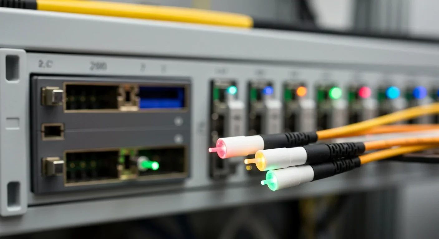
Google chose a different path. Rather than relying on centralized packet switches, TPU pods use optical circuit switches (OCS) combined with a 3D torus network topology. Think of it less like internet routing and more like old telephone switchboards - physical connections between chips that create direct optical paths with essentially zero latency.
Each TPU chip in the v7 generation has four Inter-Chip Interconnect (ICI) links providing 9.6 Tbps of aggregate bidirectional bandwidth. That's slightly less than Nvidia's latest offering, but here's the crucial difference: Google's approach scales more efficiently. A single OCS unit can handle 144×144 ports, allowing fault-tolerant routing around hardware failures without introducing packet-switching overhead.
"Optical circuit switching creates direct, low-latency optical paths between TPU chips, minimizing signal conversion losses."
- NextBigFuture Technical Analysis
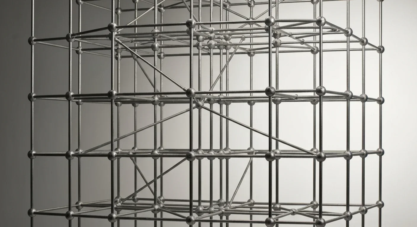
The topology itself is elegant. Chips are arranged in 4×4×4 cubes of 64 TPUs, forming a three-dimensional mesh where each chip connects to its neighbors. The 3D torus design means that, unlike flat network architectures, maximum hop count between any two chips remains low even as pod size grows. This architecture eliminates the need for high-performance packet switches while keeping inter-chip communication latency under one microsecond.
Google uses MEMS (micro-electro-mechanical systems) devices in their optical switches - tiny mirrors that physically redirect laser beams to create circuit paths. This mechanical approach uses 40% less power and costs 30% less than equivalent electrical switches. Better yet, networking costs represent less than 5% of total pod capital expenditure and less than 3% of power consumption. That's the kind of efficiency advantage that matters when you're connecting nearly 10,000 chips.
Connecting 9,216 chips is one thing; making them work together efficiently is another entirely. When a model trains across a TPU pod, the system needs to coordinate parallel operations, synchronize model updates, manage data flow, and handle inevitable hardware failures - all without introducing bottlenecks that would waste expensive compute cycles.
Google's approach centers on software-defined networking (SDN) that dynamically reconfigures the optical connections between chips. Unlike static network topologies, the OCS switches can reshape the network to match workload requirements. Training a massive transformer model with heavy all-reduce operations? The network reconfigures for optimal collective communication patterns. Running inference across multiple smaller models? The pod can partition into independent slices, each handling different workloads.
This flexibility enables mixed parallelism strategies within a single pod. Data parallelism distributes batches across chips, tensor parallelism splits individual layers across processors, and pipeline parallelism stages different model components on different hardware - all simultaneously, with the network topology adapting to support whichever communication pattern dominates at any moment.
TPU pods achieve sub-microsecond global all-reduce operations by leveraging 3D torus topology and optical circuit switching - data traverses optimal paths with minimal hop count and predictably low latency.
The software stack that orchestrates this complexity includes XLA (Accelerated Linear Algebra), Google's compiler that optimizes TensorFlow and JAX operations for TPU hardware. XLA doesn't just translate model code into chip instructions; it analyzes the entire computational graph and makes decisions about how to partition work across the pod, how to stage communications, and how to overlap computation with data transfers.
When a training job runs, each TPU chip handles a slice of the model and a portion of the training data. During the forward pass, activations flow through the network. During backpropagation, gradients are computed locally, then synchronized across chips using collective communication primitives like all-reduce. This synchronization is where interconnect bandwidth becomes critical - if gradient synchronization takes too long, expensive compute units sit idle waiting for network operations to complete.
TPU pods achieve what Google calls "sub-microsecond global all-reduce operations" by leveraging the 3D torus topology and optical circuit switching. Data traverses the mesh along optimal paths with minimal hop count, and because the connections are circuit-switched optical links rather than packet-routed networks, latency remains predictably low even under heavy traffic.
Raw performance numbers tell part of the story. A single TPU v7 chip delivers 4.6 petaFLOPS of dense FP8 performance, slightly edging out Nvidia's B200 GPU at 4.5 petaFLOPS. That represents a tenfold increase over TPU v5p, which managed 459 teraFLOPS per chip. Scale that across a 9,216-chip pod, and you reach over 42 exaflops of aggregate computational power.
But comparing chip specs misses the larger point. What matters for AI training is sustained performance during real workloads, and that depends heavily on how efficiently the system handles communication overhead, manages memory bandwidth, and keeps processors fed with data.
Google's internal benchmarks suggest TPU v4 delivered 5-87% better performance than Nvidia A100 GPUs on machine learning benchmarks, depending on the workload. More recent comparisons indicate that TPU v6 achieves 60-65% better energy efficiency than comparable GPUs, with earlier generations showing 40-45% efficiency advantages.
"TPU v6 is 60-65% more efficient than GPUs, prior generations 40-45%"
- Former Google Employee, Energy Efficiency Analysis
Energy efficiency might sound like a secondary concern, but when you're operating pods that draw approximately 10 megawatts of power, efficiency translates directly into operating costs and infrastructure constraints. TPU v7 achieves 2x better performance per watt than TPU v4, and is 30x more power-efficient than the first-generation Cloud TPU released in 2018.
Memory architecture plays a crucial role in these efficiency gains. Each Ironwood chip includes 192 GB of HBM3e memory delivering 7.4 TB/s of bandwidth. That's six times the memory capacity of TPU v4, enabling the chips to handle larger models and datasets without constantly transferring data between chip memory and external storage.
The systolic array design contributes to efficiency as well. Unlike GPUs, which evolved from graphics processors and include substantial hardware for texture processing, rasterization, and other graphics-specific tasks, TPUs are purpose-built for matrix multiplication. The systolic array loads data once, passes it through a grid of multipliers and accumulators, and produces results without writing intermediate values back to memory. This reduces memory traffic and improves operations per joule.
The true measure of infrastructure isn't theoretical performance - it's what people actually build with it. TPU pods have powered some of the most computationally intensive AI projects in history.
Google trained Gemini, its flagship large language model, on TPU infrastructure. The same pods handled training for PaLM, BERT, and T5 - models that defined state-of-the-art natural language processing at various points in AI's evolution. When Google needed to process billions of images for Google Photos or understand text in Street View imagery, TPU pods handled the inference workloads.
AlphaGo, the system that defeated world Go champion Lee Sedol in 2016, ran on first-generation TPUs. AlphaZero, which mastered chess, shogi, and Go through self-play without human-provided training data, used later generations. These projects required not just raw computational power but the ability to coordinate complex reinforcement learning algorithms across distributed hardware.
The Ironwood generation specifically targets inference-first workloads - deploying trained models at scale to handle user queries. This shift reflects the maturation of the AI industry. Early TPU generations prioritized training because model development was the bottleneck. Now, as models grow larger and deployment costs dominate, optimizing for inference has become equally critical.
Running Gemini inference on Ironwood pods achieves latency under 5 milliseconds, enabling responsive conversational AI at scale. That performance comes from the combination of high chip throughput, low-latency interconnects, and software optimizations that minimize overhead between user query and model response.
Beyond Google's internal workloads, Cloud TPU customers use pods for diverse applications: training recommendation systems, developing new language models, running large-scale simulations, processing genomic data, and accelerating scientific research. The flexibility to partition pods into smaller slices makes TPUs accessible even for organizations that don't need all 9,216 chips at once.
Understanding TPU pod capabilities matters more if you're considering actually using one. Google offers TPU access through Google Cloud Platform, with pricing that reflects the hardware's capabilities and Google's strategic positioning against Nvidia-dominated alternatives.
As of Q2 2025, TPU v5p pricing sits at $4.20 per chip-hour on-demand, or $1.89 per chip-hour with a three-year commitment. For a full 8,960-chip v5p pod, that translates to roughly $37,632 per hour on-demand, or $16,934 per hour with long-term commitment. Those numbers sound staggering until you compare them to equivalent GPU infrastructure and consider the efficiency advantages.
A former Google Cloud employee noted: "If I were to use eight H100s versus using one v5e pod, I would spend a lot less money on one v5e pod" to achieve similar model accuracy.
One former Google Cloud employee offered this perspective: "If I were to use eight H100s versus using one v5e pod, I would spend a lot less money on one v5e pod" to achieve similar model accuracy. The cost advantage stems from several factors: higher performance per watt means lower electricity costs, better networking means less time wasted on communication overhead, and purpose-built architecture means more of your budget goes toward actual computation rather than hardware features you don't need for AI workloads.
Google's Jupiter datacenter network, which connects TPU pods to the broader infrastructure, provides multi-petabit-per-second bandwidth, enabling customers to scale across multiple pods when necessary. Theoretically, Google's network could support clusters of up to 43 TPU v7 pods - roughly 400,000 accelerators working in concert. Whether such massive deployments actually exist remains closely guarded, but the infrastructure to support them is apparently in place.
The economics work differently for Google's internal usage. By building custom silicon and controlling the entire stack from chips to networking to software, Google avoids the margin that Nvidia extracts from GPU sales. This vertical integration contributes to Google's ability to target 50% margin targets in its cloud business while potentially undercutting GPU-dependent competitors on price.
TPU pod evolution shows consistent patterns: each generation roughly doubles chip performance, increases interconnect bandwidth, and expands maximum pod size. TPU v2 supported 256-chip pods; v4 reached 4,096; v7 tops out at 9,216. If that trajectory continues, TPU v8 might support 18,000+ chips per pod, creating supercomputers that would dwarf today's largest systems.
But simply making pods bigger faces physical and practical limits. Power requirements already demand liquid cooling for ~10 MW pods. Doubling pod size means doubling power infrastructure, cooling capacity, and datacenter footprint. At some point, the engineering challenges of building larger monolithic pods may push development toward better multi-pod coordination instead.
The shift toward inference-first architecture in Ironwood suggests another evolution path. As AI model deployment becomes more economically significant than training, future TPU generations might bifurcate: specialized training chips that maximize throughput for batch learning workloads, and separate inference chips optimized for latency, power efficiency, and concurrent user serving.
Networking remains a critical frontier. Google has progressively increased interconnect bandwidth from 600 GB/s in v2 to over 7.37 TB/s in v5, and now 9.6 Tbps in v7. As model sizes grow and training techniques like mixture-of-experts increase communication requirements, networking could again become the bottleneck that constrains what's possible.
The existence of TPU pods challenges several prevailing narratives about AI infrastructure. First, it demonstrates that GPU dominance isn't inevitable - purpose-built accelerators can match or exceed GPU performance while using less power and offering better economics for specific workloads.
Second, it shows that vertical integration still matters in computing. Google's ability to co-design chips, networking, software frameworks, and datacenter infrastructure gives it advantages that companies buying commodity GPUs can't easily replicate. That suggests we might see more custom silicon from major AI companies rather than universal convergence on Nvidia hardware.
Third, it highlights how architectural decisions made years ago compound over time. Google's early choice to build systolic arrays, invest in optical networking, and develop custom compilers now pays dividends as model sizes explode and training costs become prohibitive for many organizations.
The competitive implications extend beyond Google. As training costs rise and inference becomes central to AI business models, companies with efficient custom infrastructure gain structural advantages. If Google can serve AI queries at half the operating cost of competitors using GPU infrastructure, that efficiency gap could prove as significant as algorithmic improvements or model quality.
For researchers and practitioners outside these massive organizations, TPU pods represent both promise and challenge. On one hand, Cloud TPU access democratizes supercomputing - you can rent time on infrastructure that matches the world's largest supercomputers. On the other hand, the economics still favor those with deep pockets and sustained computational needs rather than academic researchers or startups experimenting with new ideas.
The fundamental engineering achievement shouldn't be overlooked amid strategic considerations. Building a system where 9,216 chips coordinate seamlessly, where optical switches route petabits of data with microsecond latency, where software automatically partitions workloads across thousands of processors - that's hard. The fact that such systems work reliably enough to trust them with months-long training runs representing millions of dollars in compute costs demonstrates how far distributed systems engineering has advanced.
We're living through an era when the infrastructure required to train frontier AI models resembles the infrastructure that once powered nuclear physics simulations or weather forecasting - massive, specialized, expensive systems that only a handful of organizations can afford to build and operate. TPU pods are Google's answer to that challenge, and their evolution will help determine what becomes computationally possible as we push toward ever-larger models and more ambitious AI applications.
The next time you interact with an AI system trained on hundreds of billions of parameters, responding in milliseconds to complex queries, remember there's a good chance its training happened inside a three-dimensional mesh of thousands of silicon chips, connected by lasers and mirrors, coordinated by software that treats 10,000 processors as a single computational engine. That's the infrastructure enabling AI's current trajectory, and Google's TPU pods show what engineering at this scale actually looks like.

Saturn's moon Titan may harbour liquid water beneath its frozen crust, kept from freezing by ammonia acting as a natural antifreeze. New Cassini data suggests the interior could be slush with warm water pockets rather than a global ocean, and NASA's Dragonfly mission launching in 2028 aims to investigate whether this exotic environment could support life.
The cerebellum, long dismissed as merely a motor coordinator, forms dense circuits with the prefrontal cortex that shape cognition and emotion. Disruption of these pathways is now linked to schizophrenia, autism, and ADHD, opening new frontiers in diagnosis and non-invasive brain stimulation therapies.
Research shows the sharing economy often increases total resource consumption through the Jevons paradox and rebound effects. Ride-sharing adds billions of vehicle miles, co-working spaces use more energy per worker, and diffused responsibility erodes conservation behavior. Breaking the paradox requires congestion pricing, accountability design, and matching sharing models to appropriate resource types.

Illusory superiority causes most people to rate themselves above average in driving, intelligence, and ethics. This bias is rooted in metacognitive blind spots, shaped by culture, and carries real costs in healthcare, finance, and leadership. Structured feedback and institutional safeguards can help, but require ongoing effort.

Eastern skunk cabbage generates its own body heat through the alternative oxidase pathway, maintaining temperatures up to 35°C above freezing air and melting surrounding snow. This thermogenic ability, shared by roughly 90 plant species worldwide, reveals a level of metabolic sophistication that challenges assumptions about plant passivity.

America has 28 vacant homes for every homeless person, yet homelessness hit record highs in 2024. Speculative investment, geographic mismatches, and political barriers explain the paradox, while Finland and Vienna show that Housing First and social housing models can work when the political will exists.
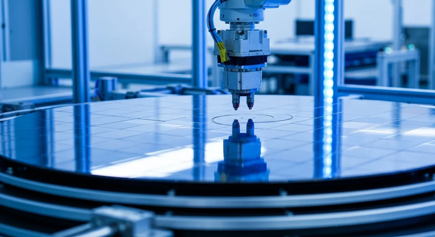
Wafer-on-wafer bonding fuses logic and memory silicon at the atomic level, delivering up to 100x interconnect density over traditional packaging. TSMC, Intel, and Samsung are racing to commercialize the technology as AI chips hit the memory bandwidth wall.

Loading featured articles...