Wafer-on-Wafer Bonding Breaks AI's Bandwidth Wall
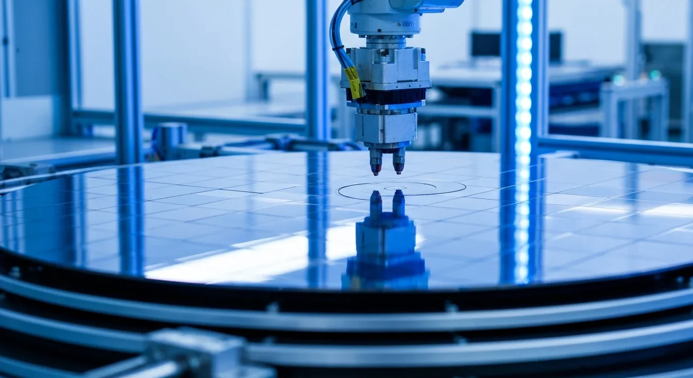
Wafer-on-Wafer Bonding Breaks AI's Bandwidth Wall
Why Quantum Computers Need 1,000 Qubits for One
TPM 2.0 and Pluton: Hardware Root of Trust Explained
Why Quantum Computing Bet on One Qubit Design
P4 Programmable Switches Rewriting Networks at Tbps
Intel TSX Failed. Can ARM Fix Transactional Memory?
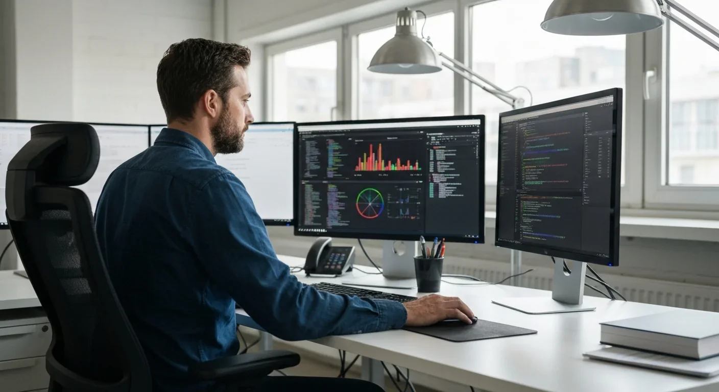
TL;DR: Google's Tensor Processing Unit revolutionized AI computing by designing specialized chips around systolic arrays that excel at matrix multiplication. TPUs achieve 2-3× better energy efficiency than GPUs through architectural innovations.
In 2016, Google quietly deployed a new kind of chip that would reshape the entire AI industry. While the world debated whether artificial intelligence would ever match human capabilities, Google's engineers were solving a different problem: the computers running AI were fundamentally wrong for the job. Traditional processors, whether CPUs or GPUs, were designed for general computing tasks. But machine learning has a specific obsession - multiplying enormous grids of numbers, billions of times per second. Google's Tensor Processing Unit wasn't just faster at this. It was designed to do nothing else.
What started as an internal project to speed up search queries evolved into the computational backbone of modern AI. Today, TPUs power everything from Google Search to breakthrough language models, and their architectural innovations have forced the entire semiconductor industry to rethink how we build computers for intelligence.
When deep learning emerged from academia in the early 2010s, researchers turned to gaming GPUs because they were the only affordable hardware that could handle parallel computation at scale. NVIDIA's chips could process thousands of operations simultaneously - perfect for rendering realistic explosions in video games, and coincidentally useful for training neural networks.
But there was an architectural mismatch. GPUs are flexible general-purpose processors designed to handle graphics, physics simulations, and compute workloads. They achieve this versatility through complex control logic, large caches, and sophisticated memory hierarchies. When you run a neural network on a GPU, maybe 30-40% of the chip's area is actually doing useful math. The rest manages scheduling, fetches data, and coordinates thousands of small processing cores.
Google's engineers recognized something crucial: neural network training and inference follow extremely predictable patterns. Unlike video games, where every frame presents new challenges, a neural network performs the same mathematical operation - matrix multiplication - billions of times in exactly the same way. This repetitive predictability is normally considered boring in computer science. For Google's hardware team, it was an opportunity.
The heart of every TPU is something called a systolic array - a grid of thousands of simple arithmetic units that work like a choreographed assembly line. The name comes from biology: just as your heart's systolic rhythm pumps blood through your body, data flows rhythmically through these processing grids.
In a TPU's systolic array, data flows through the grid like water through irrigation channels, getting reused thousands of times and eliminating nearly all memory access bottlenecks.
Here's how it's fundamentally different from a GPU. In a GPU, each core fetches its own data from memory, performs a calculation, writes the result back, then waits for new instructions. Memory access is the bottleneck - processors spend most of their time idle, waiting for data to arrive. In a TPU's systolic array, data flows through the grid like water through irrigation channels. Each processing element receives data from its neighbors, performs one multiplication, adds the result to the passing stream, and passes everything along to the next element.
This architecture eliminates almost all memory access. Data enters the array once and gets reused thousands of times as it flows through. The processing elements are tiny - each one just multiplies two numbers and adds the result to an accumulator. No complex control logic, no cache coherence protocols, no instruction decoding. Just dense arithmetic happening continuously.
The first-generation TPU, deployed in 2016, packed a 256×256 systolic array - 65,536 multiply-accumulate units working in perfect synchronization. This delivered 92 teraops of computation in a chip drawing just 40 watts. Compared to contemporary GPUs, this was 15-30 times more efficient for inference workloads. The specialized design meant TPUs could achieve 2-3× better performance per watt than GPUs for AI tasks.
Raw computational power means nothing if you can't feed it data fast enough. This is where High Bandwidth Memory becomes critical.
Standard computer memory sits on the circuit board, connected to the processor through narrow channels. High Bandwidth Memory stacks multiple memory chips vertically and places them directly next to the processor, connected through thousands of microscopic wires. It's like the difference between getting water through a garden hose versus a fire hydrant.
TPU v4 chips integrate 32GB of HBM with 1.2TB/s of bandwidth - enough to stream the entire Library of Congress in about 20 seconds. But the real innovation isn't just bandwidth, it's how the memory integrates with the systolic array architecture. Because the processing elements reuse data as it flows through the grid, the TPU can achieve effective memory bandwidth that's 10-20 times higher than what's measured at the HBM interface.
This architectural synergy between processing and memory represents the core philosophy of TPU design: optimize the entire system for one specific computation pattern, and the efficiency gains compound.
The TPU story isn't about one breakthrough chip - it's about systematic refinement of a specialized architecture as AI workloads evolved.
TPU v1 (2016) was inference-only. Google built it to run trained models faster and cheaper. It succeeded spectacularly: AlphaGo used TPUs to defeat world champion Lee Sedol, processing board positions 100 times faster than with GPU clusters.
TPU v2 (2017) added training capabilities and quadrupled performance to 180 teraflops per chip. More importantly, Google designed TPU v2s to work in pods of 256 chips interconnected with custom high-speed links. This pod architecture delivered 11.5 petaflops - the kind of computational power previously requiring warehouse-scale GPU installations.

TPU v3 (2018) doubled performance again and introduced liquid cooling to handle the thermal output of dense pod configurations. TPU v3 pods scaled to 1024 chips, delivering over 100 petaflops. This enabled Google researchers to train models that were simply impractical on GPU infrastructure.
TPU v4 (2021) brought another architectural leap: each chip now delivered 275 teraflops, and v4 pods containing 4,096 chips broke the exaflop barrier - one quintillion floating-point operations per second. To put this in perspective, the world's fastest supercomputer in 2008 achieved one petaflop. A single TPU v4 pod delivers 1,000 times that performance, in a fraction of the space.
"A single TPU v4 pod breaks the exaflop barrier - delivering 1,000 times the performance of the world's fastest supercomputer from just 15 years earlier, in a fraction of the space."
- Google Cloud Technical Documentation
TPU v5e (2023) optimized for cost-efficiency in inference workloads, achieving 2× better performance per dollar compared to v4. This matters because while training large models gets attention, 99% of actual AI compute happens during inference - billions of users making search queries, getting recommendations, translating text.
Hardware means nothing without software that can use it. Google developed the XLA (Accelerated Linear Algebra) compiler to translate high-level framework code into optimized TPU instructions.
XLA takes neural network operations written in TensorFlow or JAX and performs sophisticated optimizations: fusing multiple operations into single kernels, optimizing memory layouts, scheduling operations to maximize systolic array utilization. The compiler understands the TPU architecture intimately and can achieve performance that handwritten assembly would struggle to match.
This matters because AI researchers shouldn't need to be hardware experts. With XLA, you write your model in Python, and the compiler figures out how to map it efficiently to thousands of specialized processing elements. The TPU software stack abstracts away architectural complexity while still delivering near-optimal performance.
More recently, Google extended TPU support to PyTorch through the XLA bridge, recognizing that the ML community uses diverse frameworks. vLLM's unified backend now supports both JAX and PyTorch on TPUs, making it easier for developers to deploy large language models without rewriting their code.
TPUs dominate specific workloads, particularly training and serving large transformer models. The top machine learning models that run faster on TPUs include BERT, GPT variants, T5, and Vision Transformers - exactly the architectures driving today's AI breakthroughs.
Why? These models are characterized by enormous matrix multiplications with predictable data access patterns. They also benefit from high-bandwidth memory to handle multi-billion parameter models. TPU architecture is optimized precisely for this combination.
But TPUs aren't universal solutions. Their fixed-function design makes them less flexible for experimental architectures or non-standard operations. If your model requires custom CUDA kernels or unusual data flows, GPUs offer more programmability. For traditional computer vision or reinforcement learning with diverse operation types, GPUs often perform better.
TPUs are available exclusively through Google Cloud, while NVIDIA GPUs work anywhere. For organizations prioritizing infrastructure independence, this vendor lock-in is a critical consideration.
There's also a broader strategic consideration. TPUs are available exclusively through Google Cloud, while NVIDIA GPUs work anywhere. For organizations prioritizing infrastructure independence, this vendor lock-in matters. Some engineers compare choosing TPUs over GPUs to choosing a specialized tool that's brilliant for specific jobs but limiting if your needs change.
The efficiency advantages of specialized hardware compound dramatically at scale. Google's Ironwood TPU, their latest inference-focused design, achieves nearly 30× better energy efficiency than first-generation TPUs. In practical terms, this means running the same AI service with one-thirtieth the electricity and cooling infrastructure.
When you're serving billions of queries daily, those efficiency gains translate to massive environmental and economic impacts. If every major AI company achieved similar efficiency improvements, the projected energy consumption of AI could drop from concerning to manageable. Data centers running TPUs can deliver AI services at a fraction of the carbon footprint of equivalent GPU installations.

Cost efficiency follows similar math. Cloud customers report 4× better performance per dollar on TPU v6e compared to GPU alternatives for specific workloads. This democratizes AI development - smaller teams can train meaningful models without enterprise-scale infrastructure budgets.
TPU's success sparked an industry-wide shift. Amazon developed Trainium and Inferentia, Microsoft invested in custom AI accelerators, and startups like Cerebras and Graphcore pursued even more radical architectural innovations. The era of one-size-fits-all processors is ending.
This specialization reflects a broader trend in computing. For decades, general-purpose CPUs got faster through transistor scaling and higher clock speeds. That era ended around 2005 when power consumption became the limiting factor. The industry responded with parallel processing - multi-core CPUs and then GPUs. Now we're entering a new phase: domain-specific architectures where different types of computation get their own optimized silicon.
Neural networks get TPUs. Database queries might get purpose-built data analytics chips. Video encoding gets specialized media processors. This heterogeneous computing future promises order-of-magnitude efficiency improvements, but it also fragments the industry. Developers must understand multiple architectures and frameworks must target diverse hardware.
The proof of TPU's impact lives in production systems handling real-world scale. Google Search uses TPUs to understand query intent and rank billions of pages in milliseconds. Google Photos processes trillions of images for face recognition and object detection. Google Translate handles over 100 billion words daily, with neural translation models running on TPU infrastructure.
DeepMind's AlphaFold 2, which solved the protein folding problem and won a Nobel Prize in Chemistry, relied heavily on TPU v3 pods for training. The computational breakthrough required weeks of continuous computation across hundreds of chips - exactly the kind of sustained, predictable workload where TPUs excel.
"DeepMind's AlphaFold 2 solved the 50-year-old protein folding problem using TPU v3 pods running continuously for weeks - a computational feat that earned a Nobel Prize in Chemistry."
- Network World Technical Analysis
Gmail's Smart Compose feature generates contextual sentence completions for over 1.5 billion users. The inference demands require low latency (users notice delays over 100ms) combined with massive throughput. TPUs deliver both through specialized design: the systolic array processes each request efficiently, while pod architecture handles millions of simultaneous users.
NVIDIA hasn't stood still. Their H100 and upcoming B200 chips incorporate transformer-specific optimizations and compete directly with TPUs on AI workloads. The performance gap is narrowing, and NVIDIA's ecosystem advantage - millions of developers familiar with CUDA, comprehensive libraries, and hardware available everywhere - remains formidable.
Google's response is TPU v7, rumored to feature even more aggressive architectural specialization. Industry analysts speculate about innovations like sparse computation acceleration, mixture-of-experts optimization, and tighter integration between chips in pod configurations. The TPU v7 architecture could represent Google's most significant challenge to NVIDIA's datacenter dominance yet.
But the competitive dynamic is complex. NVIDIA succeeds by being available to everyone; Google keeps TPUs mostly internal or cloud-only to maintain competitive advantage. This means TPU innovations often remain invisible to the broader developer community until competitors copy the concepts.
The TPU story reveals a fundamental shift in how we should think about computational efficiency. For fifty years, computer architecture prioritized flexibility. General-purpose processors that could run any program were considered superior to specialized chips. This made sense when software diversity was high and transistor budgets were limited.
But now we have billions of transistors to work with, and AI workloads represent a massive, uniform computation pattern executed trillions of times daily. In this context, the economics favor specialization. A TPU's systolic array might only do one thing, but it does that one thing with extraordinary efficiency.
This principle extends beyond AI. We're seeing similar specialization in cryptography (Bitcoin mining ASICs), networking (programmable switches), and storage (computational storage drives). The future of computing isn't one better processor - it's diverse specialized processors orchestrated by intelligent compilers and frameworks.
The second lesson is about memory and computation co-design. TPU's performance doesn't come from faster arithmetic - it comes from eliminating wasted time moving data around. Modern processors spend more energy moving bits than computing with them. Future architectures must obsess over data locality and memory hierarchy, not just raw computational throughput.
For AI practitioners, the TPU vs GPU decision isn't about which is "better" - it's about matching architecture to workload. If you're training transformers at scale, deploying production inference at high volume, or working within Google Cloud's ecosystem, TPUs offer compelling advantages in performance and cost.
If you need maximum flexibility, are prototyping novel architectures, require specific CUDA libraries, or want hardware independence, GPUs remain the practical choice. Many organizations use both: GPUs for research and experimentation, TPUs for production deployment of validated models.
The emergence of framework-agnostic TPU backends and improved tooling is reducing the switching cost. Developers can increasingly write model code once and target different hardware depending on deployment requirements. This portability represents the maturation of AI infrastructure from experimental chaos to engineering discipline.
Beyond technical specifications and benchmark comparisons, TPUs represent something more fundamental: the transformation of AI from academic curiosity to industrial infrastructure. The decision to build custom silicon reflected Google's belief that machine learning would become as essential as databases or networking - important enough to warrant dedicated hardware.
That bet has proven correct. AI isn't a specialized application anymore; it's becoming the default interface for human-computer interaction. Search, recommendations, content creation, code generation, scientific discovery - all increasingly powered by neural networks running on specialized accelerators.
The companies controlling AI infrastructure - the chips, frameworks, and cloud platforms - wield disproportionate influence over which AI applications get built and who can build them.
This creates both opportunity and risk. The companies controlling AI infrastructure - the chips, frameworks, and cloud platforms - wield disproportionate influence over which AI applications get built and who can build them. Google's TPU advantage helps maintain their dominance in search and cloud AI services. Amazon's Trainium and Microsoft's custom chips serve similar strategic purposes.
For the broader tech ecosystem, this matters. If training cutting-edge models requires access to TPU pods or similar infrastructure, AI capabilities become concentrated among a few large organizations. Open-source models and academic research must either settle for smaller scales or depend on cloud platforms they don't control.
The next generation of AI accelerators will likely push specialization even further. Sparse computation - where most neural network parameters are zero - enables 10-100× efficiency improvements with appropriate hardware support. Mixture-of-experts models activate different specialized sub-networks for different inputs, requiring smart routing logic in silicon.
Analog computing, where calculation happens through physical properties of materials rather than digital logic, promises another order-of-magnitude leap in energy efficiency. Photonic accelerators using light instead of electricity could eventually deliver petaflops-scale computation in chip-scale packages.
But the fundamental insight behind TPU architecture will endure: when you have a computation pattern that's repetitive, predictable, and performed at massive scale, specialized hardware beats general-purpose processors by enormous margins. The future of computing is diverse silicon ecosystems, where different tasks run on different optimized architectures.
For developers and organizations navigating this transition, the strategic question isn't which hardware will "win" - it's how to architect systems that can leverage specialized accelerators while maintaining flexibility as both hardware and algorithms evolve. The teams that figure this out will build AI applications that are not just more capable, but radically more efficient and accessible.
The TPU revolution isn't just about faster matrix multiplication. It's about reimagining what computers should be when the work we need them to do fundamentally changes. And if the first decade of specialized AI hardware delivered this much progress, the next decade promises transformations we're only beginning to imagine.

Saturn's moon Titan may harbour liquid water beneath its frozen crust, kept from freezing by ammonia acting as a natural antifreeze. New Cassini data suggests the interior could be slush with warm water pockets rather than a global ocean, and NASA's Dragonfly mission launching in 2028 aims to investigate whether this exotic environment could support life.
The cerebellum, long dismissed as merely a motor coordinator, forms dense circuits with the prefrontal cortex that shape cognition and emotion. Disruption of these pathways is now linked to schizophrenia, autism, and ADHD, opening new frontiers in diagnosis and non-invasive brain stimulation therapies.
Research shows the sharing economy often increases total resource consumption through the Jevons paradox and rebound effects. Ride-sharing adds billions of vehicle miles, co-working spaces use more energy per worker, and diffused responsibility erodes conservation behavior. Breaking the paradox requires congestion pricing, accountability design, and matching sharing models to appropriate resource types.

Illusory superiority causes most people to rate themselves above average in driving, intelligence, and ethics. This bias is rooted in metacognitive blind spots, shaped by culture, and carries real costs in healthcare, finance, and leadership. Structured feedback and institutional safeguards can help, but require ongoing effort.

Eastern skunk cabbage generates its own body heat through the alternative oxidase pathway, maintaining temperatures up to 35°C above freezing air and melting surrounding snow. This thermogenic ability, shared by roughly 90 plant species worldwide, reveals a level of metabolic sophistication that challenges assumptions about plant passivity.

America has 28 vacant homes for every homeless person, yet homelessness hit record highs in 2024. Speculative investment, geographic mismatches, and political barriers explain the paradox, while Finland and Vienna show that Housing First and social housing models can work when the political will exists.
Wafer-on-wafer bonding fuses logic and memory silicon at the atomic level, delivering up to 100x interconnect density over traditional packaging. TSMC, Intel, and Samsung are racing to commercialize the technology as AI chips hit the memory bandwidth wall.

Loading featured articles...